Pulsed laser single particle testing device and testing method for bare chip

A pulsed laser and test device technology, applied in the direction of measuring devices, electronic circuit testing, non-contact circuit testing, etc., can solve the problems of increasing the uncertainty of test results, fewer components, and the inability to quantitatively evaluate the incident laser energy loss, etc., to achieve Save development costs, avoid damage, and ensure smooth progress

Inactive Publication Date: 2018-04-06
CHINA ACADEMY OF SPACE TECHNOLOGY
View PDF6 Cites 3 Cited by
  • Summary
  • Abstract
  • Description
  • Claims
  • Application Information

AI Technical Summary

Problems solved by technology

[0005] The single event effect simulation test based on the existing pulsed laser test conditions mainly has the following two shortcomings: First, after the conventional device is uncapped, there is a metal layer on the front of the chip, which will block the incident laser light. Due to the reflection and scattering of the metal layer, the incident Laser energy loss cannot be quantitatively evaluated, thus increasing the uncertainty of test results; second, there are only a few flip-chip devices at present, and the device can be directly incident after the cap is removed, but the substrate thickness of the device needs to be measured in advance to calculate the effective laser incident energy. Accurately evaluate the anti-single particle ability of the device, but there are relatively few such devices, and the engineering promotion of the pulsed laser simulation single particle test method still needs to be prepared for the applicability test sample

Method used


Image

  • Pulsed laser single particle testing device and testing method for bare chip
  • Pulsed laser single particle testing device and testing method for bare chip

Examples


Embodiment 1

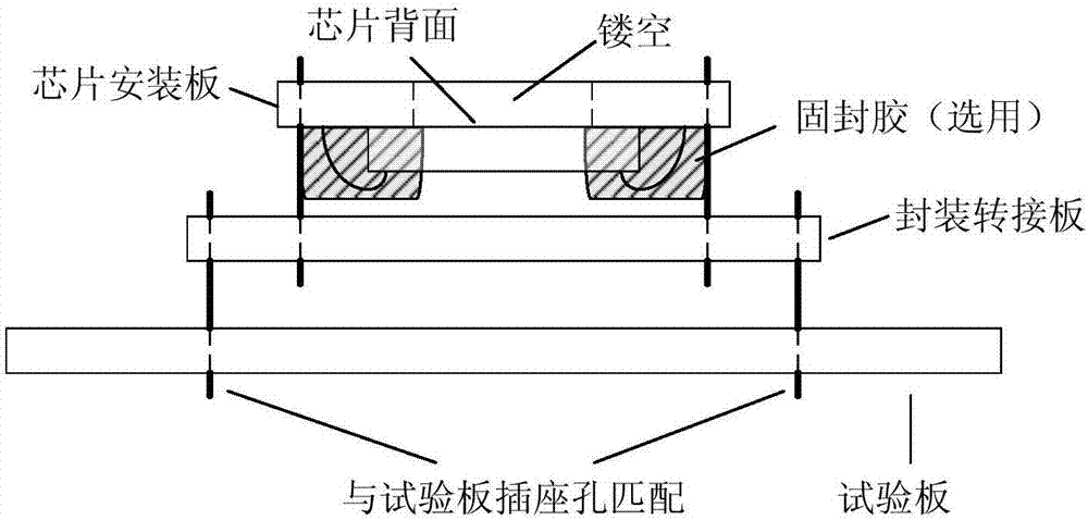
[0067] Such as figure 1 As shown, a pulsed laser single particle test device for a bare chip, the device includes a chip mounting board, a packaging adapter and a test board;

[0068] The chip mounting board is used to fix the PROM chip to be tested. The metal wiring area of ​​the chip is 0.4mm×1.5mm, and the chip is diced into a size of 0.8mm×2mm. The area should be larger than the metal wiring area of ​​the chip to be tested, and the chip scribing size should be larger than the hollow area. The back of the chip to be tested is fixed on the lower surface of the chip mounting board with glue around the back, and the back of the chip to be tested is bonded to the lower surface of the chip mounting board; the chip to be tested is facing down, and the hollow through holes are arranged according to the arrangement of the solder joints of the chip to be tested Corresponding pads and corresponding pins are used as lead-out pins. Bonding wires are used to make sequential electrical ...

Embodiment 2

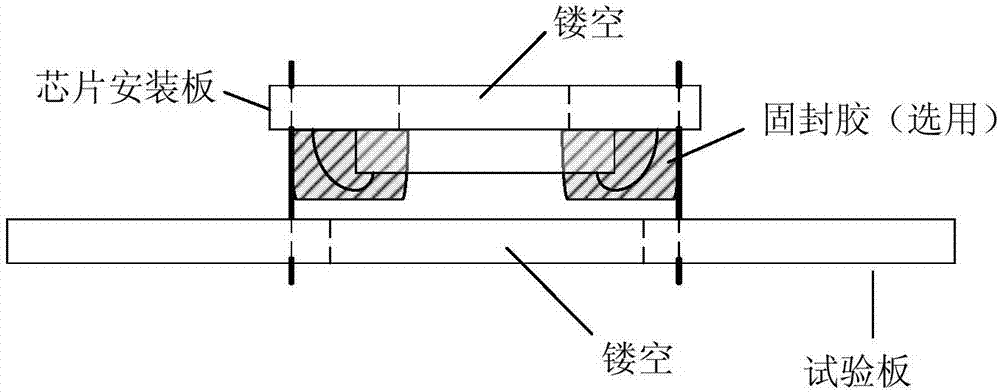
[0071] Such as figure 2 As shown, a pulsed laser single particle test device for a bare chip, the device includes a chip mounting board and a test board;

[0072] The chip mounting plate is used to fix the CMOS image sensor chip to be tested. The metal wiring area of ​​the chip is 1.5mm×4.5mm, and the chip is diced to a size of 2.1mm×5.1mm. The hollow area in the center of the chip mounting plate is designed to be 1.8mm ×4.8mm, the hollowed out area should be larger than the metal wiring area of ​​the chip to be tested, and the chip scribing size should be larger than the hollowed out area. The back of the chip to be tested is fixed and installed on the lower surface of the chip mounting plate with glue, and the back of the chip to be tested is attached to the lower surface of the chip mounting plate; pad, and there are pins electrically connected to the pad as lead-out pins, the solder joints of the chip to be tested and the pad are electrically connected sequentially with ...


PUM


Abstract

The invention relates to a pulsed laser single particle testing device and a testing method for a bare chip, which belong to the technical field of semiconductor device anti-space single particle effect ability detection. Pads made on a chip mounting board and chip welding points are in sequential correspondence and are connected through bonding wires, the back surface of the chip faces upwards and is fit with the chip mounting board, the front surface of the device faces downwards, the bonding wire is immobilized through an immobilization adhesive, the chip and the bonding wire are thus in astable state, the center hollow area of the chip mounting board can expose the back surface of the chip, and when the mounting board is arranged on a clamp through leading-out pins, the hollow area faces upwards, the back surface of the chip faces upwards, and thus, the back surface incidence requirement in the pulsed laser single particle test can be met. The test can be ensured to be smoothly carried out, and effectiveness of a test result can be ensured.

Description

technical field [0001] The invention relates to a pulsed laser single particle test device and a test method of a bare chip, and belongs to the technical field of semiconductor device anti-space single particle effect detection technology. Background technique [0002] When a semiconductor device is used in a space environment, space high-energy particles will penetrate the interior of the semiconductor device and generate ionization on the path, and the circuit nodes will absorb the electrons and holes generated by the ionization to cause errors. This effect is called single event effect. The ability to verify the anti-single event effect of semiconductor devices on the ground mainly relies on ground heavy ion accelerators to simulate single event experiments, but the resources of heavy ion accelerators are limited. The machine time for carrying out single event experiments on aerospace components is far from meeting the demand. Pulsed laser simulation of single event effe...

Claims


Application Information

Patent Timeline
Patent Type & Authority Applications(China)
IPC IPC(8): G01R31/28G01R31/311
CPCG01R31/2856G01R31/311
Inventor 罗磊李晓亮梅博于庆奎张洪伟孙毅吕贺莫日根
Owner CHINA ACADEMY OF SPACE TECHNOLOGY
Why Eureka
Try Eureka