

PCB circuit board structure and manufacturing process thereof
A kind of PCB circuit board, manufacturing process technology, applied in the direction of printed circuit, printed circuit parts, electrical components, etc., can solve the problems of PCB circuit board electronic components damage, PCB circuit board damage, large generation and other problems, to reduce temperature, prevent Moisture, avoid damage effect
- Summary
- Abstract
- Description
- Claims
- Application Information
AI Technical Summary
Problems solved by technology
Method used
Image

Examples
Embodiment Construction
[0016] The following will clearly and completely describe the technical solutions in the embodiments of the present invention with reference to the accompanying drawings in the embodiments of the present invention. Obviously, the described embodiments are only some, not all, embodiments of the present invention. Based on the embodiments of the present invention, all other embodiments obtained by persons of ordinary skill in the art without making creative efforts belong to the protection scope of the present invention.
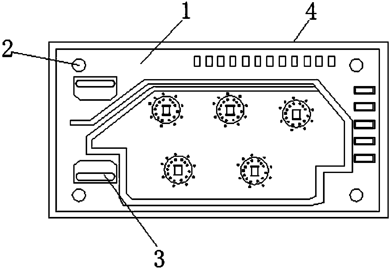
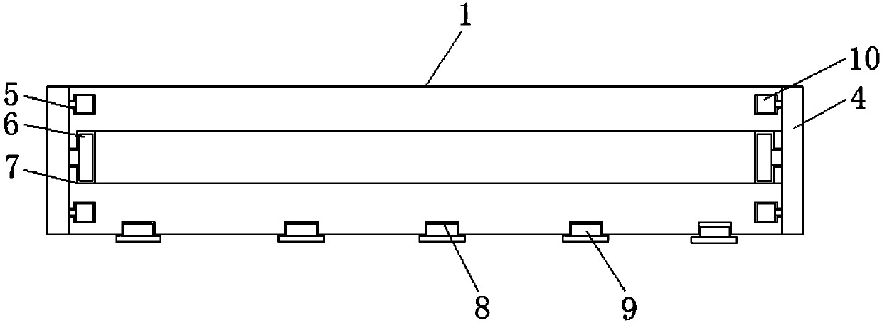
[0017] see figure 1 , figure 2 and image 3 , the present invention provides a technical solution: a PCB circuit board structure and its manufacturing process, including a board body 1, the upper surface of the board body 1 is provided with fixing holes 2 around, and the upper surface of the board body 1 is provided with mounting holes 3, The outer side of the board body 1 is provided with a waterproof cover 4, the peripheral surface of the board body 1 is ...
PUM
 Abstract
Description
Claims
Application Information