GOA circuit

A circuit and potential technology, applied in the direction of instruments, static indicators, etc., can solve the problems of reducing device life, short scanning signal waveform, threshold voltage shift, etc., and achieve the goal of improving device life, shortening falling time, and reducing electrical stress Effect

Active Publication Date: 2018-04-13
SHENZHEN CHINA STAR OPTOELECTRONICS SEMICON DISPLAY TECH CO LTD
View PDF7 Cites 16 Cited by
  • Summary
  • Abstract
  • Description
  • Claims
  • Application Information

AI Technical Summary

Problems solved by technology

The structure of this GOA circuit is simple, and the space for fan-out routing (Layout) is small, but with the improvement of screen resolution and frequency, it is necessary to shorten the falling time (Falling time) of the scanning signal waveform. Consider increasing the voltage difference between the low potential of the clock signal CK' and the potential of the first low potential signal VSS1, the larger the voltage difference, the shorter the falling time of the scanning signal waveform, but in figure 1 Under the architecture of the GOA circuit shown, increasing the voltage difference between the low potential of the clock signal CK' and the potential of the first low potential signal VSS1 increases the ripple (Ripple) of the scanning signal G(N)' output by the GOA circuit. , affecting the display effect
[0007] To solve this problem, in the prior art, the sources of the forty-first thin film transistor T41', the forty-second thin film transistor T42', and the forty-third thin film transistor T43' are usually connected to the first low potential signal VSS1 is connected to a second low potential signal whose potential is the same as the low potential of the clock signal CK', which can solve the problem caused by the increase in the voltage difference between the low potential of the clock signal CK' and the potential of the first low potential signal VSS1. The problem of the increase of the ripple of the scanning signal G(N)', but because the voltage difference between the potential of the first low potential signal VSS1 and the low potential of the clock signal CK' is very large, and the potential of the second low potential signal and the clock The low potential of the signal CK' is the same, the forty-first thin film transistor T41' in the pull-down module 300' will be in the forward bias for a long time, so that the threshold voltage of the forty-first thin film transistor T41' will shift seriously, reduce device lifetime

Method used


Image

  • GOA circuit
  • GOA circuit
  • GOA circuit

Examples


Embodiment Construction

[0035] In order to further illustrate the technical means adopted by the present invention and its effects, the following describes in detail in conjunction with preferred embodiments of the present invention and accompanying drawings.

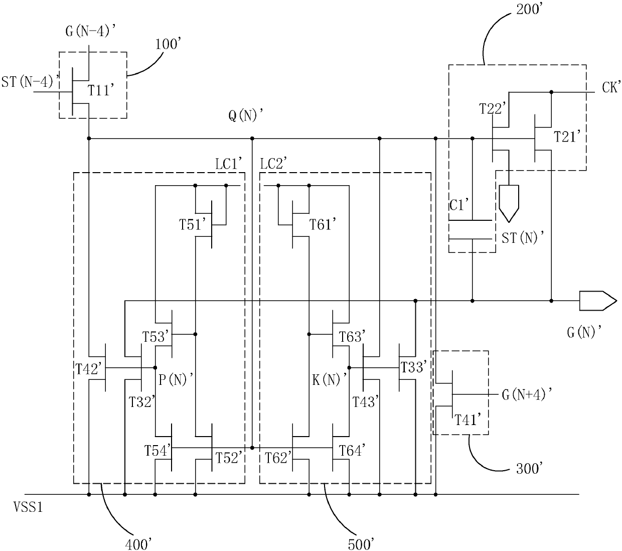
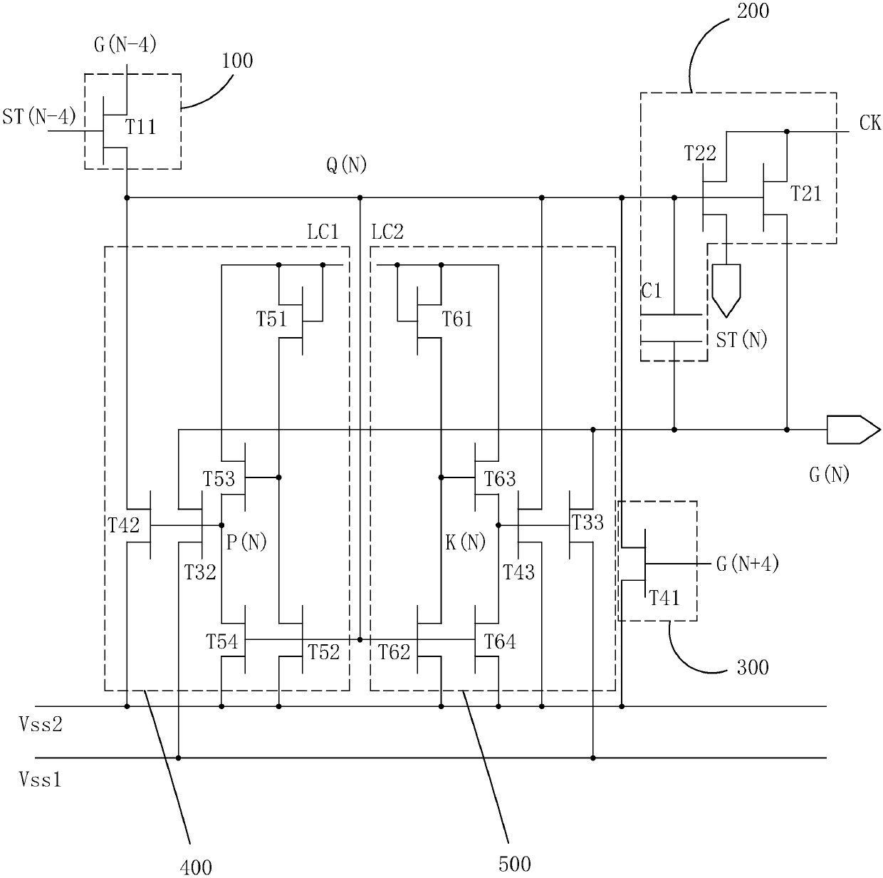
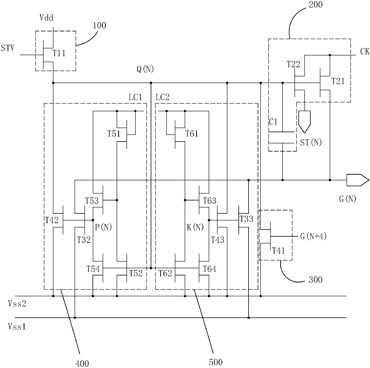
[0036] The present invention provides a GOA circuit, please refer to figure 2 , is a circuit diagram of an embodiment of the GOA circuit of the present invention, the GOA circuit of the present invention includes: a multi-level GOA unit, and each level of GOA unit includes: a pull-up control module 100, an output module 200, a pull-down module 300, a first A pull-down maintenance module 400, and a second pull-down maintenance module 500;

[0037] Let N be a positive integer, except for the GOA units from the first level to the fourth level and the GOA units from the penultimate level to the last level, in the N-level GOA units:

[0038] The pull-up control module 100 is connected to the transmission signal ST(N-4) of the N-4th GOA unit of th...


PUM


Abstract

The invention provides a GOA circuit. Each level of GOA unit of the GOA circuit comprises a pull-up control module, an output module, a pull-down module, a first pull-down maintaining module and a second pull-down maintaining module. The gates of the thirty-second thin film transistor in the first pull-down maintaining module and the thirty-third thin film transistor in the second pull-down maintaining module are electrically connected with second and third nodes respectively. The sources all access a first low-potential signal. The drains all access a scan signal. The sources of the forty-second thin film transistor in the first pull-down maintaining module, the forty-third thin film transistor in the second pull-down maintaining module, and the forty-first thin film transistor in the pull-down module access a second low-potential signal. The potential of the first low-potential signal is greater than the potential of the second low-potential signal. The potential of the second low-potential signal is greater than the low potential of a clock signal. The falling time of the scan signal is shortened, and at the same time the electrical stress of the thin film transistor in the pull-down module can be reduced.

Description

technical field [0001] The invention relates to the field of display technology, in particular to a GOA circuit. Background technique [0002] A Liquid Crystal Display (LCD) has many advantages such as a thin body, power saving, and no radiation, and has been widely used. Such as: LCD TV, mobile phone, personal digital assistant (PDA), digital camera, computer screen or notebook computer screen, etc., occupy a dominant position in the field of flat panel display. [0003] Most of the liquid crystal displays currently on the market are backlight liquid crystal displays, which include a liquid crystal display panel and a backlight module. The working principle of the liquid crystal display panel is to pour liquid crystal molecules between the thin film transistor array substrate (ThinFilm Transistor Array Substrate, TFT Array Substrate) and the color filter substrate (ColorFilter, CF), and apply a driving voltage on the two substrates to Control the rotation direction of the...

Claims


Application Information

Patent Timeline
Patent Type & Authority Applications(China)
IPC IPC(8): G09G3/36
CPCG09G3/3677
Inventor 吕晓文陈仁禄
Owner SHENZHEN CHINA STAR OPTOELECTRONICS SEMICON DISPLAY TECH CO LTD
Why Eureka
Try Eureka