Supercharge Your Innovation With Domain-Expert AI Agents!

Thin film flip chip packaging structure

A chip packaging structure and thin-film flip-chip technology, applied in electrical components, electrical solid devices, circuits, etc., can solve the problems of connecting bumps, not connecting to bumps, poor bonding accuracy between chips and flexible circuit substrates, etc. Achieve the effect of improving joint quality and easy judgment

Inactive Publication Date: 2018-04-17
CHIPMOS TECH INC
View PDF4 Cites 0 Cited by
  • Summary
  • Abstract
  • Description
  • Claims
  • Application Information

AI Technical Summary

Problems solved by technology

However, at present, there is no graphic or image displayed on the chip and the flexible circuit substrate for the machine to calculate and judge the joint angle and position between the chip and the flexible circuit substrate, resulting in the gap between the chip and the flexible circuit substrate. The bonding accuracy is poor, and it is difficult to accurately arrange each pin of the flexible circuit carrier in the center of the corresponding bump
Furthermore, pins may be incompletely connected to bumps, not connected to bumps, or connected to wrong bumps due to chip offset

Method used


Image

  • Thin film flip chip packaging structure
  • Thin film flip chip packaging structure
  • Thin film flip chip packaging structure

Examples


Embodiment Construction

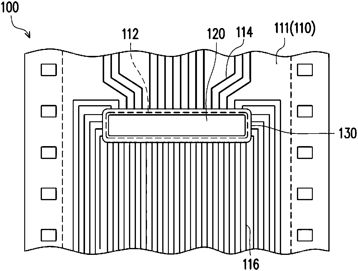
[0036] figure 1 It is a schematic partial top view of a thin-film flip-chip packaging structure according to an embodiment of the present invention. see figure 1 , the thin film flip chip packaging structure 100 of this embodiment includes a flexible circuit carrier 110 and a chip 120 . The flexible circuit carrier 110 includes a flexible substrate 111 and a circuit structure 113 disposed on the flexible substrate 111 . The flexible substrate 111 is, for example, a part of a film roll. The flexible substrate 111 includes a chip bonding area 112 .

[0037] figure 2 yes figure 1 A partial bottom view of the thin-film flip-chip packaging structure with the flexible substrate hidden. image 3 yes figure 2 A partially enlarged schematic diagram. In order to clearly describe the connection relationship between the bumps of the chip 120 and the pins on the flexible circuit carrier 110, figure 2 The arrangement of the bumps on the active surface of the chip 120 and the rel...


PUM


Abstract

The invention provides a thin film flip chip packaging structure, including a flexible circuit carrier and a chip. The flexible circuit carrier includes a flexible substrate and a circuit structure configured on the flexible substrate, the flexible substrate includes a chip bonding area, the circuit structure includes a plurality of pins and at least one virtual pin, each of the pins has an innerpin part located in the chip bonding area, and the at least one pin has an alignment pattern located in the chip bonding area. The chip includes a plurality of bumps and at least one virtual bump, thechip is configured in the chip bonding area, so that the bumps are connected with the inner pin parts respectively, the alignment pattern of the at least one virtual pin corresponds to the at least one virtual bump, and orthographic projection of the alignment pattern on the chip at least locally surrounds the at least one virtual bump and a gap G exists between the orthographic projection and the edge of the at least one virtual bump. The thin film flip chip packaging structure provided by the invention can accurately bond the bumps of the chip to the pins of the flexible circuit carrier.

Description

technical field [0001] The invention relates to a packaging structure, in particular to a film flip-chip packaging structure. Background technique [0002] With the improvement of semiconductor technology, liquid crystal displays have the advantages of low power consumption, thin and light weight, high resolution, high color saturation, and long life, so they are widely used in mobile phones, notebook computers or desktop computers. Electronic products closely related to life such as LCD screens and LCD TVs. Among them, the driver IC of the display is an indispensable and important component of the liquid crystal display. To meet the needs of various applications of driver chips for liquid crystal display devices, tape automatic bonding (TAB) packaging technology is generally used for chip packaging, and Chip-On-Film (COF) packaging structure is one of them. A packaging structure of widely used tape and tape automatic bonding technology. [0003] The thin-film flip-chip p...

Claims


Application Information

Patent Timeline
IPC IPC(8): H01L23/488H01L23/49
CPCH01L2224/73204H01L23/488H01L23/49
Inventor 陈必昌方俊凯
Owner CHIPMOS TECH INC
Features
  • R&D
  • Intellectual Property
  • Life Sciences
  • Materials
  • Tech Scout
  • Unparalleled Data Quality
  • Higher Quality Content
  • 60% Fewer Hallucinations
Learn More