Circuit board with thick copper circuit, and manufacturing method for circuit board

A manufacturing method and circuit board technology, applied in the directions of printed circuit manufacturing, printed circuits, printed circuits, etc., can solve problems such as poor etching factor, and achieve the effect of avoiding unclean etching and burr phenomenon.

Active Publication Date: 2018-04-17
AVARY HLDG (SHENZHEN) CO LTD +1
View PDF2 Cites 5 Cited by
  • Summary
  • Abstract
  • Description
  • Claims
  • Application Information

AI Technical Summary

Problems solved by technology

The line width of the conventional printed circuit board production process is limited by the thickness of the copper layer. The thinner the copper layer, the thinner the lines, so there are limitations in using thick copper to make thin lines; and the conductive lines of conventional printed circuit boards are usually reduced. It is a well-established method, but limited by the thickness of copper, it can only be used with thin copper for making thin lines, and the etching factor is poor after production, and the etching is not clean to form burrs

Method used


Image

  • Circuit board with thick copper circuit, and manufacturing method for circuit board
  • Circuit board with thick copper circuit, and manufacturing method for circuit board
  • Circuit board with thick copper circuit, and manufacturing method for circuit board

Examples


Embodiment Construction

[0033] The circuit board provided by the present invention and its manufacturing method will be further described in detail below with reference to the drawings and embodiments.

[0034] see Figure 1-15 , the first embodiment of the present invention provides a method for manufacturing a circuit board with thick copper lines, the steps of which include:

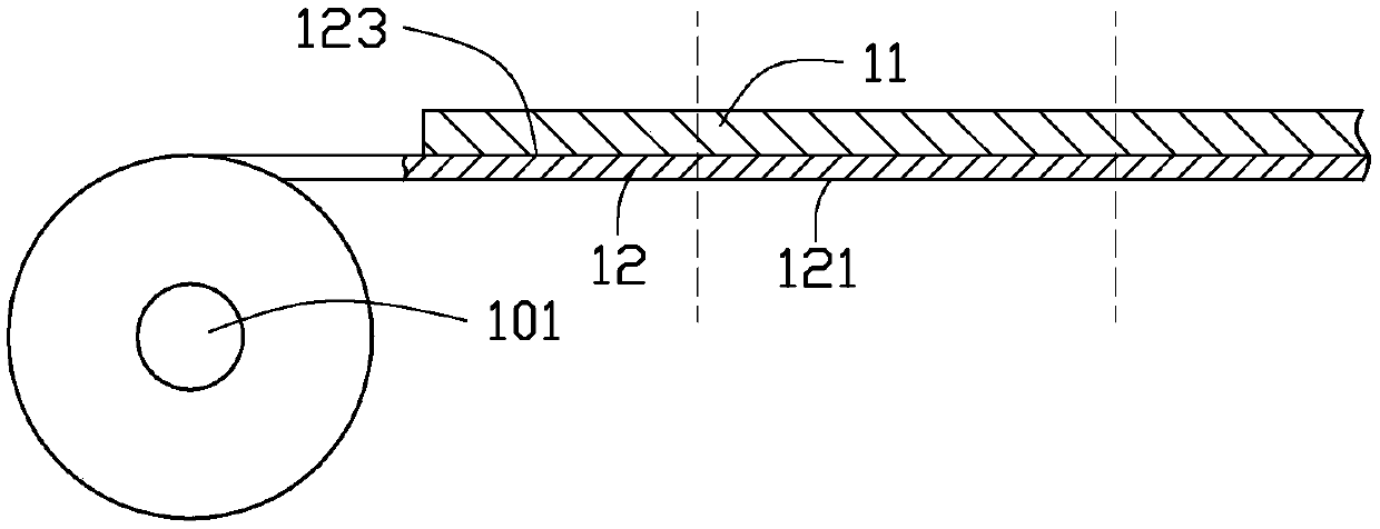
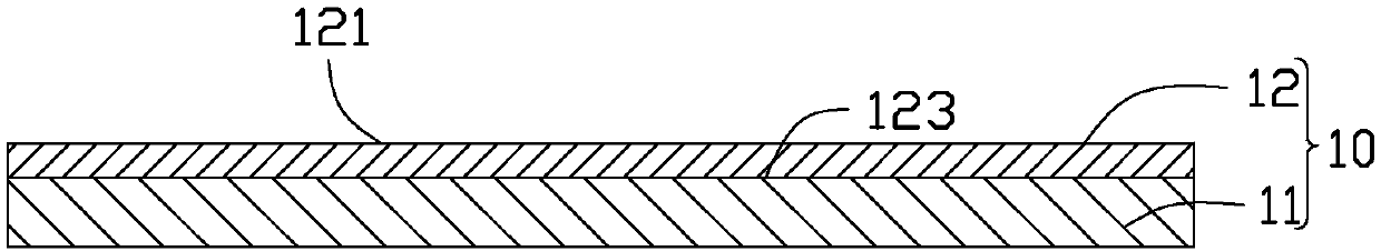
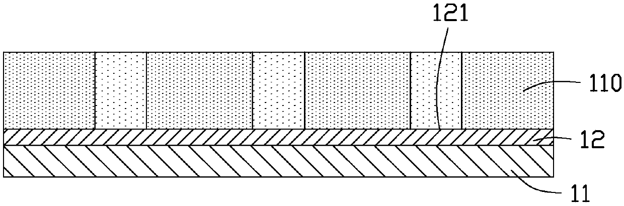
[0035] For a first step, see Figure 1 to Figure 2 , provide a single-sided copper-clad substrate 10, the single-sided copper-clad substrate 10 includes a support layer 11 and a base copper layer 12 covering the surface of the support layer 11, the base copper layer 12 includes a first surface 121 and the support layer 11 contact with the second surface 123 . The support layer 11 may be polyethylene terephthalate (PET).

[0036] The method for providing the single-sided copper-clad substrate 10 includes: see figure 1 , provide the base copper layer 12 wound on the reel 101, roll out the base copper layer 12 from the reel...


PUM

PropertyMeasurementUnit
thicknessaaaaaaaaaa
thicknessaaaaaaaaaa
thicknessaaaaaaaaaa

Abstract

The invention provides a manufacturing method for a circuit board, and the method comprises the steps: providing a copper-coated substrate which comprises a supporting layer and a base copper layer; carrying out the electroplating on one surface of the base copper layer to form a first conductive circuit diagram; forming a first protection layer on the surface of the first conductive circuit diagram, wherein the first protection layer is disposed in a gap between the first conductive circuit diagram and the base copper layer; peeling off the support layer; carrying out the electroplating on the other surface of the base copper layer to form a second conductive circuit diagram; removing the parts, which are exposed by the first and second conductive circuit diagram, of the base copper layerthrough etching, so as to enable the base copper layer to form a base copper conductive circuit diagram, wherein the base copper conductive circuit diagram and the first and second conductive circuitdiagrams jointly form a conductive circuit diagram; forming a second protection layer on the surface of the second conductive circuit diagram, wherein the second protection layer is disposed in a gapbetween the second conductive circuit diagram and the first protection layer.

Description

technical field [0001] The invention relates to the field of circuit board production, in particular to a circuit board with thick copper lines and a production method thereof. Background technique [0002] With the rapid development of electronic products, the printed circuit board as the support of components and the carrier of electrical signals should also gradually become miniaturized, lightweight, high-density and multi-functional, and then the production of fine lines of printed circuit boards put forward higher requirements. The line width of the conventional printed circuit board production process is limited by the thickness of the copper layer. The thinner the copper layer, the thinner the line, so the use of thick copper to make thin lines has its own limitations; and the conductive lines of conventional printed circuit boards are usually reduced. However, limited by the thickness of copper, only thin copper can be used to make thin lines, and the etching factor...

Claims


Application Information

Patent Timeline
Patent Type & Authority Applications(China)
IPC IPC(8): H05K1/11H05K3/06H05K3/24
CPCH05K1/11H05K3/06H05K3/243H05K2203/054Y10T29/49155H05K3/0097H05K2201/0355H05K3/064H05K3/427H05K2203/1545H05K3/108H05K2203/0152H05K1/0393H05K3/4652H05K2201/0137H05K2201/0154H05K2203/107H05K2203/0228H05K3/4682H05K1/0225H05K3/282H05K3/188H05K3/0026H05K1/111H05K1/09
Inventor 许芳波吴鹏沈鉴泉吴科建
Owner AVARY HLDG (SHENZHEN) CO LTD
Why Eureka
Try Eureka