Radiating packaging structure and manufacturing method thereof

A technology of packaging structure and heat dissipation type, which is used in semiconductor/solid-state device manufacturing, electrical components, electric solid-state devices, etc., can solve the problems of affecting the appearance of the package, large loss of cutting tools, and increased cost, so as to avoid the problem of burrs and cutting tools. Wear problems, the effect of reducing cutting costs

Inactive Publication Date: 2008-01-23
SILICONWARE PRECISION IND CO LTD
View PDF3 Cites 2 Cited by
  • Summary
  • Abstract
  • Description
  • Claims
  • Application Information

AI Technical Summary

Problems solved by technology

[0007] However, in the aforementioned semiconductor package manufacturing method, during the cutting step, because the cutting tool continues to cut through the heat sink, and because the heat sink is generally made of metal materials such as copper and aluminum, when cutting with a diamond cutting knife , will cause the peripheral material of the heat sink to produce uneven sharp-edged edges (or burrs) due to pulling, which will affect the appearance of the package, and will also cause too much loss of the cutting tool, resulting in a significant increase in cost, and the production efficiency cannot be greatly improved.

Method used


Image

  • Radiating packaging structure and manufacturing method thereof
  • Radiating packaging structure and manufacturing method thereof
  • Radiating packaging structure and manufacturing method thereof

Examples


no. 1 example

[0052] Please refer to FIGS. 4A and 4F , which are schematic diagrams of the first embodiment of the heat-dissipating package structure and its manufacturing method of the present invention.

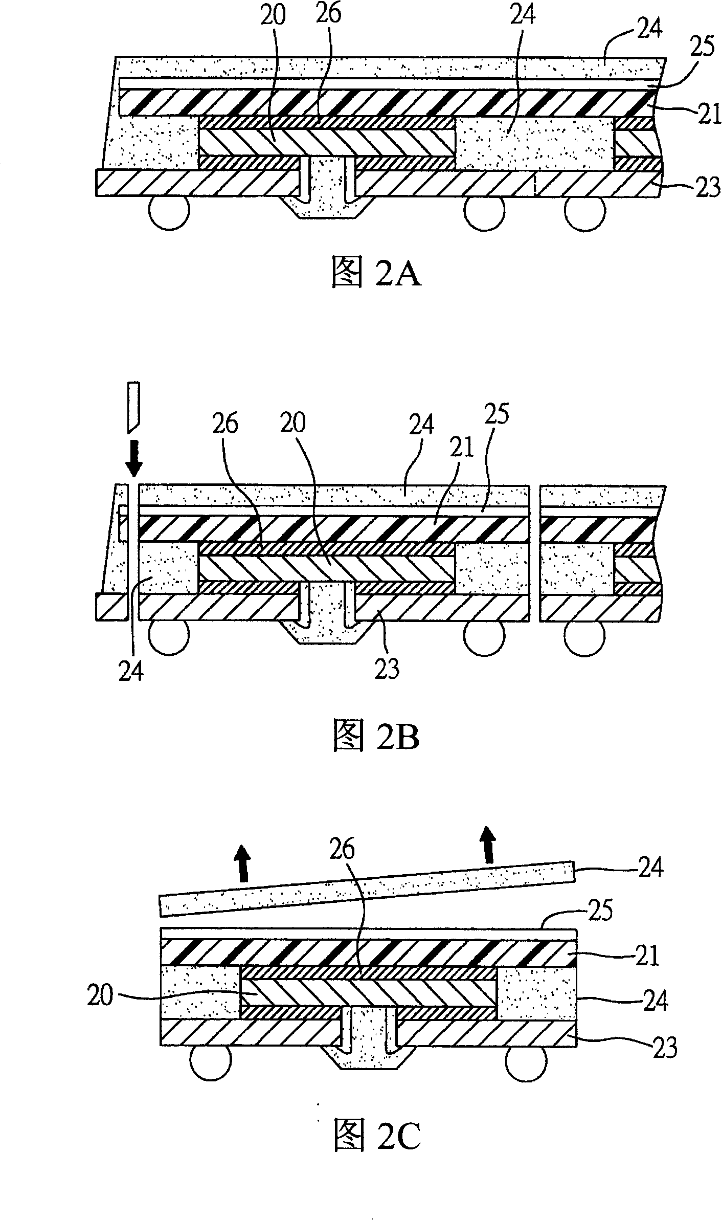
[0053] As shown in FIG. 4A , at first, the semiconductor chip 41 is placed and electrically connected to the chip carrier 42, and at the same time, a heat sink 44 with an interface layer 43 on the surface is connected to the heat sink 44 with one side of the heat sink 44. The surface of the semiconductor wafer 41 that is not provided for contact with the wafer carrier 42 . The planar dimension of the heat sink does not exceed the planar dimension of the semiconductor package structure to be formed.

[0054] The chip carrier 42 is, for example, a ball grid array (BGA) substrate or a land grid array (LGA) substrate, and the semiconductor chip 41 is, for example, a flip-chip semiconductor chip, and the flip-chip semiconductor chip is passed through a plurality of conductive bumps. 410 to e...

no. 2 example

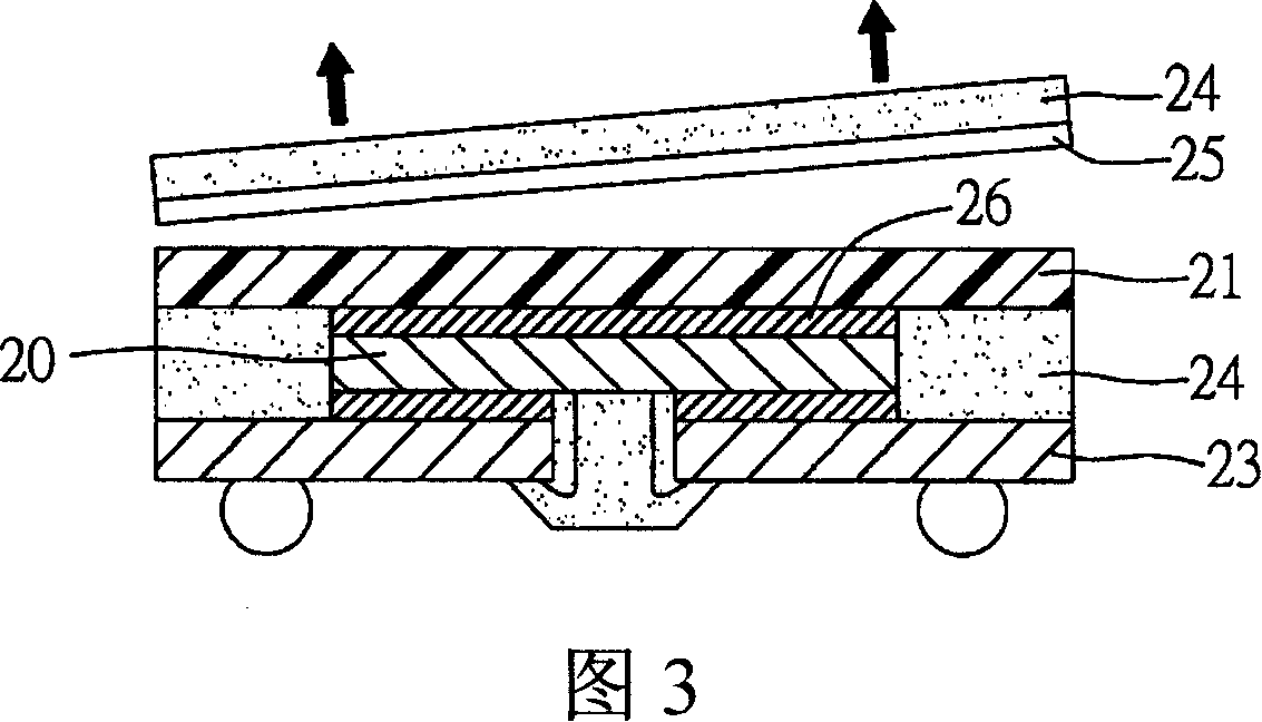
[0062] Please refer to FIGS. 5A and 5B (the FIG. 5B is a top view of FIG. 5A ), which are cross-sectional and top schematic views of the second embodiment of the heat dissipation package structure of the present invention. The manufacturing method of the heat-dissipating package structure in the second embodiment of the present invention is substantially the same as the above-mentioned manufacturing method, the main difference is that when the bevel is formed on the top edge of the sealing compound 55 by means of grinding operations, etc., the sealing compound 55 is ground and stretched. to the heat sink 54 , so as to facilitate the subsequent removal of the interface layer on the surface of the heat sink and the excess encapsulant on the interface layer.

no. 3 example

[0064] Please refer to FIG. 6 , which is a schematic cross-sectional view of the third embodiment of the semiconductor package structure made with reference to the heat dissipation type package structure method of the present invention. The difference is that in the semiconductor package structure of this embodiment, the radiator 64 is attached The material of the interface layer 63 on the surface is selected so that the bonding force with the heat sink 64 is greater than the bonding force between the interface layer 63 and the encapsulant 65', such as a metal layer such as gold or nickel, so that the cutting operation is completed along the predetermined package structure size, and After the top edge of the encapsulant 65 is ground to form a bevel, the encapsulant 65' located on the interface layer 63 can be removed from the interface layer 63 during the removal operation, so that the interface layer 63 is exposed to the package. The colloid 65 allows the heat generated by the...


PUM


Abstract

A heat dispersion encapsulation structure and its method are provided, which is characterized in that: place and connect a semiconductor wafer to a wafer bearing component; position a heat dispersion component with a interference face layer on its surface on the semiconductor wafer, so as to form a complete encapsulation glue body that wraps the semiconductor wafer and the heat dispersion component; then, cut the wafer bearing component and the encapsulation glue body according to the preset dimension of the encapsulation structure and form a bevel at the top brim of the encapsulation glue body, so as to partially expose the brim of the heat dispersion component; then, remove the encapsulation glue body on the interference face layer and form the encapsulation glue body that covers the interference face layer by keeping a spacing elevation between the encapsulation glue body and the top face of the interference face layer. Meanwhile, because the cutting path of the cutting operation does not pass the heat dispersion component, the invention is able to prevent the problem of flash and wearing of cutter due to the direct cutting of the heat dispersion component by the cutter, thus reducing the cutting cost.

Description

technical field [0001] The invention relates to a heat dissipation packaging structure and a manufacturing method thereof, in particular to a semiconductor packaging structure with heat dissipation parts and a manufacturing method thereof. Background technique [0002] With the demand for thinner, thinner and smaller electronic products, semiconductor packages integrating semiconductor chips with high-density electronic components and electronic circuits have gradually become the mainstream of packaging products. However, since the semiconductor package generates high heat during operation, if the heat of the semiconductor chip is not released immediately, the accumulated heat will seriously affect the electrical function and product stability of the semiconductor chip. On the other hand, in order to prevent the internal circuit of the package from being polluted by external water and dust, the surface of the semiconductor chip must be covered with an encapsulant to insulate...

Claims


Application Information

Patent Timeline
IPC IPC(8): H01L21/50H01L21/56H01L23/34H01L23/31
CPCH01L2224/73253H01L2224/16225
Inventor 黄建屏蔡和易曾文聪
Owner SILICONWARE PRECISION IND CO LTD
Why Eureka
Try Eureka