Wafer surface appearance control system and control method

A surface topography and control method technology, applied in semiconductor/solid-state device manufacturing, electrical components, circuits, etc., can solve process defects such as wafer surface topography changes exceeding process specifications, wafer exposure, etc., and automatically adjust wet etching etc. to achieve good surface morphology and avoid defects

Inactive Publication Date: 2018-04-20
HUAIAN IMAGING DEVICE MFGR CORP
View PDF6 Cites 7 Cited by
  • Summary
  • Abstract
  • Description
  • Claims
  • Application Information

AI Technical Summary

Problems solved by technology

[0003] In view of the shortcomings of the prior art described above, the purpose of the present invention is to provide a wafer surface topography control system and control method, which are used to solve the problem that the wet etching process after chemical mechanical polishing in the prior art cannot be based on chemical The wafer morphology after mechanical polishing automatically adjusts the wet etching process parameters. After the wafer is wet etched, it is easy to cause the morphology of the wafer surface to change beyond the process specifications, resulting in defects during wafer exposure and other processes. question

Method used


Image

  • Wafer surface appearance control system and control method
  • Wafer surface appearance control system and control method
  • Wafer surface appearance control system and control method

Examples


Embodiment 1

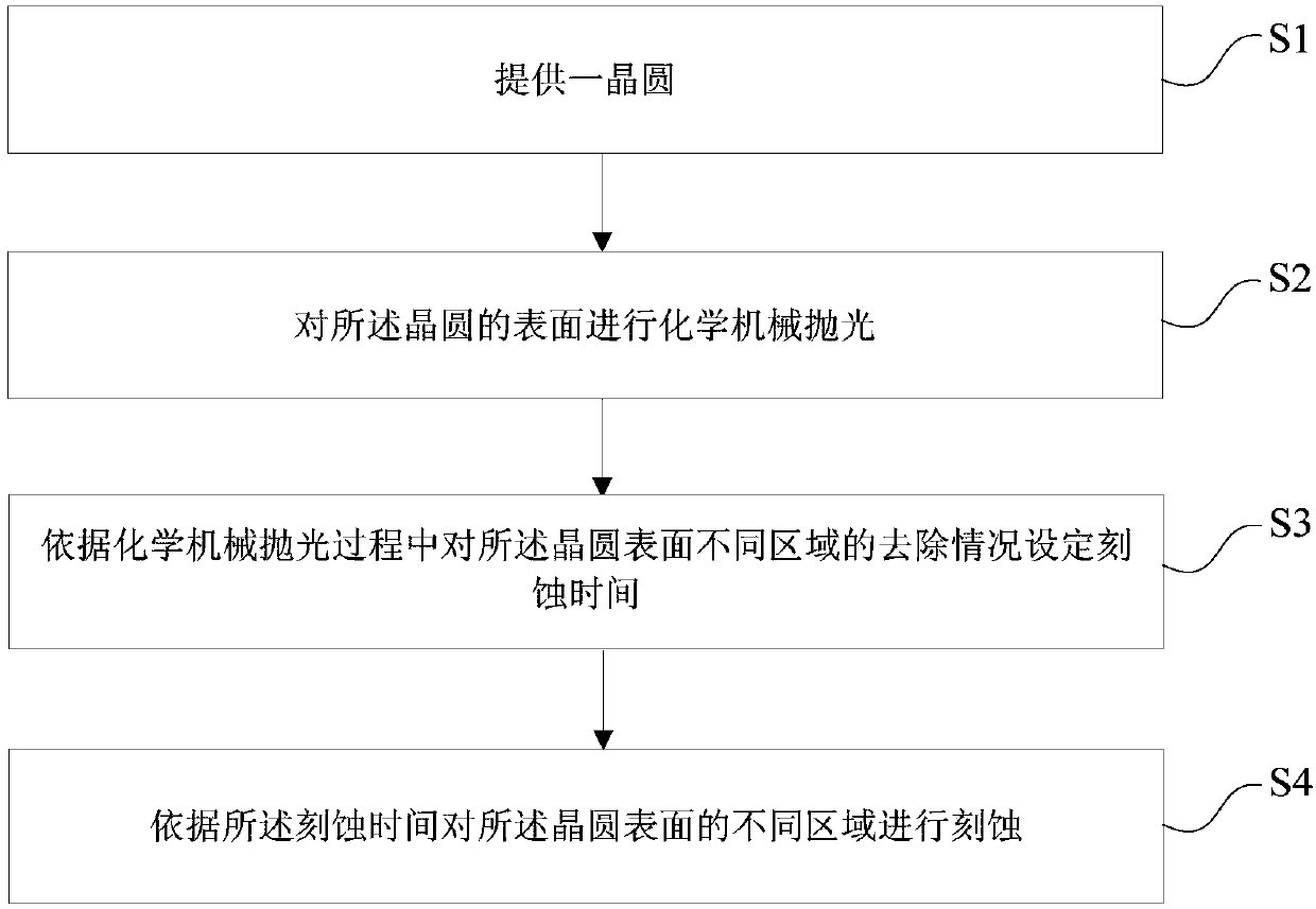
[0057] see image 3 , the present invention provides a method for controlling the surface topography of a wafer, the method for controlling the surface topography of the wafer includes the following steps:

[0058] 1) providing a wafer;

[0059] 2) Carry out chemical mechanical polishing to the surface of described wafer;

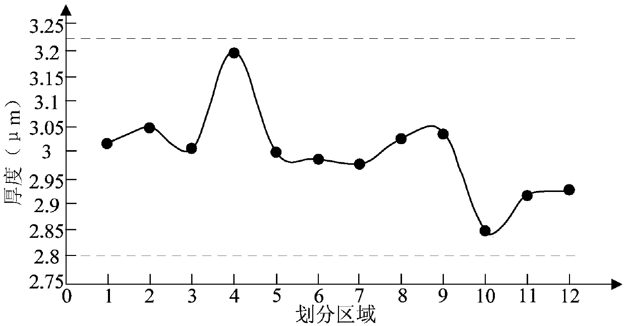
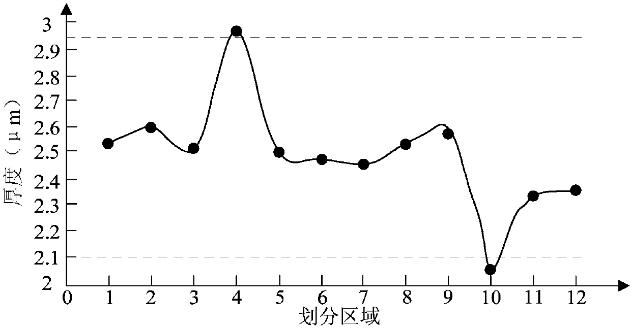
[0060] 3) setting the etching time according to the removal of different regions of the wafer surface during the chemical mechanical polishing process;

[0061] 4) Etching different regions of the wafer surface according to the etching time.

[0062] In step 1), see image 3 In step S1, a wafer is provided.

[0063] As an example, the wafer may be a silicon wafer, a sapphire wafer, or a gallium nitride wafer, etc. Preferably, in this embodiment, the wafer is a silicon wafer. A semiconductor device structure may be formed in the wafer, preferably, a back-illuminated image sensor may be formed in the wafer. Of course, in other examples, the wafer may also...

Embodiment 2

[0086] read on Figure 6 , this embodiment also provides a wafer surface topography control system, the wafer surface topography control system is used to implement the wafer surface topography control method described in Embodiment 1, the wafer surface topography The control system includes: a chemical mechanical polishing device 1, which is used to chemically mechanically polish the surface of the wafer 5; a measuring device 2, which is used to measure the chemical mechanical polishing The thickness of each region of the wafer 5; the setting module 3, the setting module 3 is connected with the measuring device 2, and is used to set the etching time according to the structure measured by the measuring device 2; An etching device 4, the etching device 4 is connected to the setting module 3, and is used to etch different regions of the surface of the chemically mechanically polished wafer 5 according to the etching time set by the setting module 3 .

[0087] As an example, th...


PUM


Abstract

The invention provides a wafer surface appearance control system and control method. The wafer surface appearance control method comprises the following steps of 1) providing a wafer; 2) performing chemical mechanical polishing on the surface of the wafer; 3) setting etching time according to removal conditions in different regions of the wafer surface in the chemical mechanical polishing process;and 4) performing etching on different regions of the wafer surface according to the etching time. The wet etching time for the wafer is set according to the removal conditions in different regions of the wafer surface in the chemical mechanical polishing process, and the appearance deviation of the wafer surface caused in the chemical mechanical polishing process in the wet etching process can be compensated, so that the wet etched wafer has high surface appearance, the wafer surface appearance is effectively controlled within the reasonable technological specifications, and generation of defects in the subsequent process can be avoided.

Description

technical field [0001] The invention relates to the technical field of semiconductors, in particular to a wafer surface topography control system and control method. Background technique [0002] The chemical mechanical polishing (CMP) process is a very important process in the semiconductor field at present, and it is widely used to correct the flatness of the wafer surface. However, after the wafer is chemically mechanically polished, there will be certain changes in the surface of the wafer, such as figure 1 As shown, the thickness of different regions on the wafer surface will vary. In the follow-up wet etching process, the existing method adopted is to spray etching liquid in the wafer with constant wet etching process parameters (for example, the etching time of different regions of the wafer, etc.). The surface of the wafer is etched, and the process parameters of wet etching are not automatically adjusted according to the wafer morphology after chemical mechanical ...

Claims


Application Information

Patent Timeline
Patent Type & Authority Applications(China)
IPC IPC(8): H01L21/306H01L21/67
CPCH01L21/30625H01L21/3065H01L21/67253
Inventor 吕新强林宗贤吴孝哲吴龙江郭松辉王海宽
Owner HUAIAN IMAGING DEVICE MFGR CORP
Why Eureka
Try Eureka