
CMOS image sensor and manufacturing method thereof

A technology of image sensor and manufacturing method, which is applied in semiconductor/solid-state device manufacturing, electric solid-state devices, semiconductor devices, etc., can solve problems such as low cost and influence on process stability, achieve convenient mass production, save photolithographic plates, and improve The effect of process stability

Inactive Publication Date: 2018-05-04
SHANGHAI HUALI MICROELECTRONICS CORP
View PDF8 Cites 0 Cited by
  • Summary
  • Abstract
  • Description
  • Claims
  • Application Information

AI Technical Summary

Problems solved by technology

[0010] In the existing process, the N-type implanted region 102 and the P-type implanted region 104 usually need to be distributed and defined by a photolithography process. 104 Alignment will have a certain impact on process stability

Method used


Image

  • CMOS image sensor and manufacturing method thereof
  • CMOS image sensor and manufacturing method thereof
  • CMOS image sensor and manufacturing method thereof

Examples


Embodiment Construction

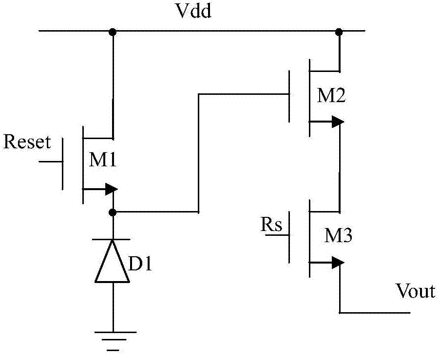
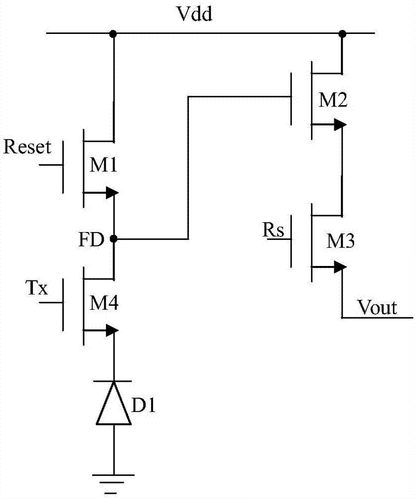
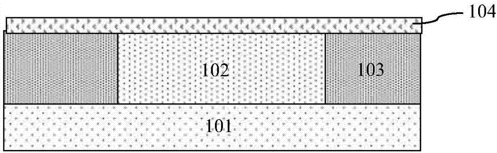
[0044] Such as Figure 5 What is shown is a schematic structural diagram of a photodiode of each pixel unit of a CMOS image sensor according to an embodiment of the present invention; each pixel unit of the CMOS image sensor provided by the present invention includes: an N-type injection region 2 and a P-type injection region 4.

[0045] The N-type implanted region 2 is formed on the surface of the P-type semiconductor substrate 1 and a PN junction diode formed between the N-type implanted region 2 and the P-type semiconductor substrate 1 serves as a photosensitive diode; Zone 2 stores photo-generated electrons after the photodiode is exposed to light.

[0046] The top surface structure of the N-type injection region 2 is circular or polygonal.

[0047] Preferably, a P-type epitaxial layer is further formed on the surface of the P-type semiconductor substrate 1, and the N-type implanted region 2 is formed in the P-type epitaxial layer. The P-type semiconductor substrate 1 is a P-typ...


PUM


Abstract

The invention discloses a CMOS image sensor. A pixel unit of the CMOS image sensor includes an N-type injection region of a photodiode and a surface P-type injection region formed on the N-type injection region. The region sizes of the P-type injection region and the N-type injection region each are provided with a self-aligned structure defined by an identical photolithographic plate, the regionsize of the P-type injection region is formed by enlarging after isotropic etchingis performed on a mask of the N-type injection region, and a mask of the N-type injection region is defined by a photolithographic plate corresponding to the N-type injection region. The invention also discloses a method for manufacturing the CMOS image sensor. According to the CMOS image sensor, one photolithographic plate can be saved, the process cost is reduced, process stability can be improved, and mass production is facilitated.

Description

Technical field [0001] The invention relates to the field of semiconductor integrated circuit manufacturing, in particular to a CMOS image sensor; the invention also relates to a manufacturing method of the CMOS image sensor. Background technique [0002] The existing CMOS image sensor (CMOS Image Sensor, CIS) is composed of a pixel unit circuit and a CMOS circuit. Compared with the CCD image sensor, the CMOS image sensor adopts the CMOS standard production process, so it has better integration and can It is integrated with other digital-analog operations and control circuits on the same chip, which is more suitable for future development. [0003] According to the number of transistors included in the pixel unit circuit of the existing CMOS image sensor, it is mainly divided into a 3T type structure and a 4T type structure. [0004] Such as figure 1 As shown, it is a schematic diagram of an equivalent circuit of a pixel unit circuit of an existing 3T CMOS image sensor; the pixel un...

Claims


Application Information

Patent Timeline
IPC IPC(8): H01L27/146H01L21/8232
CPCH01L27/14601H01L27/14643H01L27/14683H01L27/14689H01L21/8232
Inventor 梅翠玉秋沉沉曹亚民
Owner SHANGHAI HUALI MICROELECTRONICS CORP
Features
  • Generate Ideas
  • Intellectual Property
  • Life Sciences
  • Materials
  • Tech Scout
  • Unparalleled Data Quality
  • Higher Quality Content
  • 60% Fewer Hallucinations
Learn More