Welding device for power semiconductor module

A technology of power semiconductors and welding devices, which is applied in the direction of semiconductor devices, semiconductor/solid-state device components, electric solid-state devices, etc., can solve the problems of difficult expansion of welding devices, difficult release of welding stress, and low welding quality, etc., to achieve extended use Strong resistance, avoiding the accumulation of stress, and simple structure

Active Publication Date: 2018-05-08
ZHUZHOU CRRC TIMES SEMICON CO LTD
View PDF5 Cites 0 Cited by
  • Summary
  • Abstract
  • Description
  • Claims
  • Application Information

AI Technical Summary

Problems solved by technology

[0007] In view of this, the object of the present invention is to provide a power semiconductor module welding device, which solves the problems of complicated power terminal welding tooling in the existing power semiconductor module packaging process, difficulty in releasing welding stress, poor welding quality and difficulty in expanding the use of the welding device. question

Method used


Image

  • Welding device for power semiconductor module
  • Welding device for power semiconductor module
  • Welding device for power semiconductor module

Examples


Embodiment Construction

[0027] In order to make the purpose, technical solutions and advantages of the embodiments of the present invention more clear, the technical solutions in the embodiments of the present invention will be clearly and completely described below in conjunction with the drawings in the embodiments of the present invention. Apparently, the described embodiments are only some of the embodiments of the present invention, not all of them. Based on the embodiments of the present invention, all other embodiments obtained by persons of ordinary skill in the art without creative efforts fall within the protection scope of the present invention.

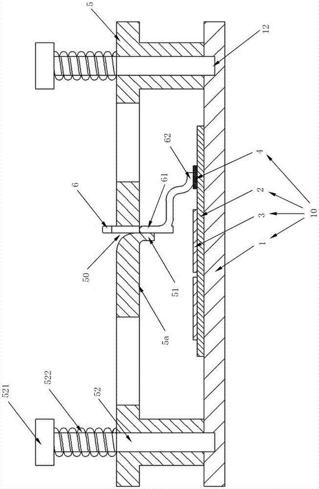
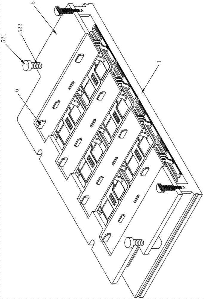
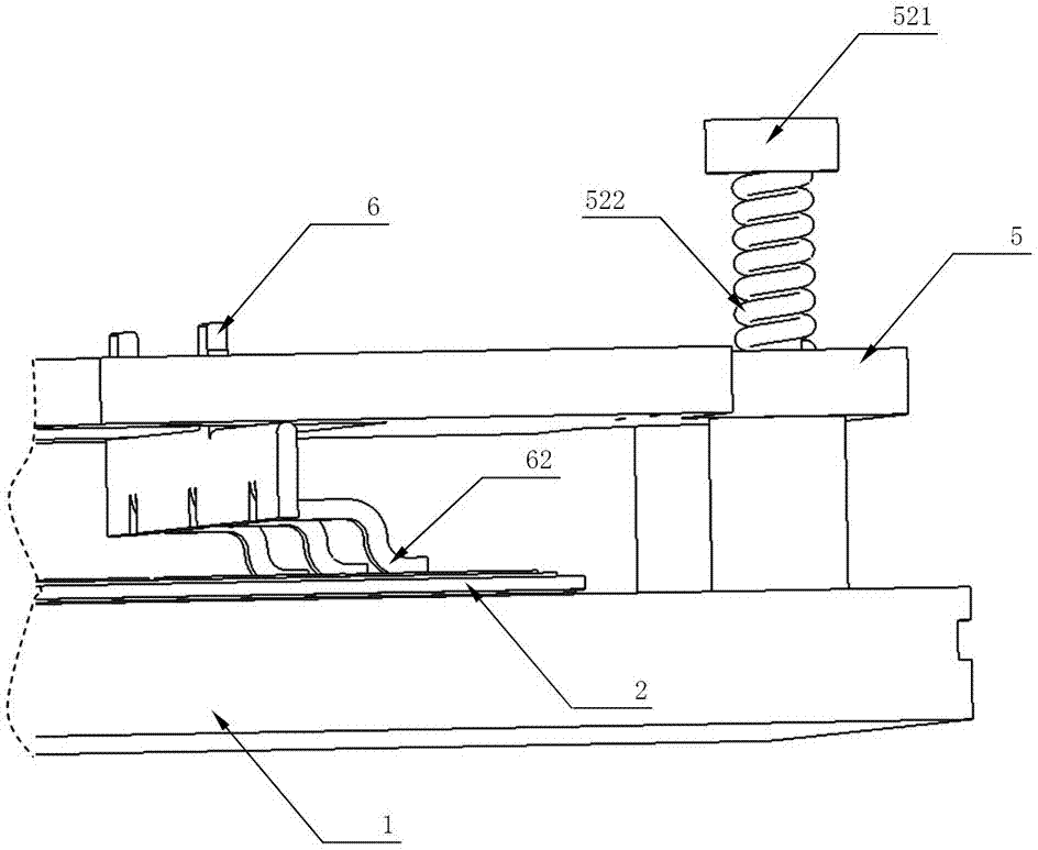
[0028] as attached figure 1 to attach image 3 As shown, specific embodiments of the power semiconductor module welding device of the present invention are given, and the present invention will be further described below in conjunction with the accompanying drawings and specific embodiments.

[0029] as attached figure 1 And attached figure ...


PUM


Abstract

The invention discloses a welding device for a power semiconductor module, and the device comprises a substrate assembly, a fixed flat plate, an elastic crimping part, and a power terminal. The substrate assembly comprises a bottom plate and an insulating part disposed on the substrate, wherein the insulating part is provided with a semiconductor chip and a welding part. The fixed flat plate is fixed on the substrate assembly through the elastic crimping part, and a space for accommodating the power terminal is formed between the fixed flat plate and the substrate assembly. The power terminalpasses through the fixed flat plate, and abuts against the lower part of the upper bottom surface of the fixed flat plate, and a pin part at the tail end of the power terminal makes contact with the welding part under the positioning effect of the fixed flat plate. The pressure adjustment of the power terminal in a fixing and welding process is achieved through the elastic crimping part. The device can solve technical problems that the welding quality is not high and a welding device is difficult to extend because a power terminal in the conventional packaging technology of power semiconductormodules is complex in welding tool and the welding stress is difficult to release.

Description

technical field [0001] The invention relates to the field of power electronic device manufacturing, in particular to a welding device with a pressure regulating function applied to a power semiconductor module. Background technique [0002] At present, the packaging process of power semiconductor modules, such as IGBT (Insulated Gate Bipolar Transistor, ie insulated gate bipolar transistor) modules, usually involves multiple times of welding. The welding of power terminals and substrate components is usually the last welding, and it is also the most critical process in the entire packaging process, because the welding quality is directly related to the service life and reliability of the module. At present, although advanced power semiconductor module packaging technology can realize accurate positioning and welding operations of a small number of power terminals and substrate components, with the sharp increase in power density, high-power semiconductor modules are facing h...

Claims


Application Information

Patent Timeline
Patent Type & Authority Applications(China)
IPC IPC(8): H01L23/32H01L25/07
CPCH01L25/072H01L23/32
Inventor 袁勇黄南陈燕平熊辉时海定文驰孙康康高海祐
Owner ZHUZHOU CRRC TIMES SEMICON CO LTD
Why Eureka
Try Eureka