Liquid crystal display panel and display device

A liquid crystal panel and display device technology, applied in optics, instruments, electrical components, etc., can solve the problems of complex liquid crystal panel process, reduce user experience, increase production cost, etc., to improve user experience, eliminate stage difference, and increase screen occupation. the effect of

Inactive Publication Date: 2018-05-29
HUIZHOU CHINA STAR OPTOELECTRONICS TECHNOLOGY CO LTD
View PDF8 Cites 20 Cited by
  • Summary
  • Abstract
  • Description
  • Claims
  • Application Information

AI Technical Summary

Problems solved by technology

[0003] At present, the borderless design of liquid crystal displays is usually to extend the color filter (Color filter, that is, color filter) from one side of the substrate of the lower end of the array (ThinFilm Transistor array, TFT for short) in the liquid crystal panel. , referred to as CF) substrate, set the Bonding (bonding) terminal on the extension part to connect the driver chip to the printed circuit board, because after bonding, the circuit device in the bonding area will cause reflection problems, so it is necessary to print the extension area processing makes the frameless LCD panel process complicated and increases the production cost. In addition, because the binding end generally requires a certain width, although there is no physical frame visually in this case, the binding end in the viewing surface The width exists and is wide, which reduces the user experience

Method used


Image

  • Liquid crystal display panel and display device
  • Liquid crystal display panel and display device
  • Liquid crystal display panel and display device

Examples


Embodiment Construction

[0020] In order to make the object, technical solution and advantages of the present invention more clear, the present invention will be further described in detail below in conjunction with the accompanying drawings and embodiments. It should be understood that the specific embodiments described here are only used to explain the present invention, not to limit the present invention.

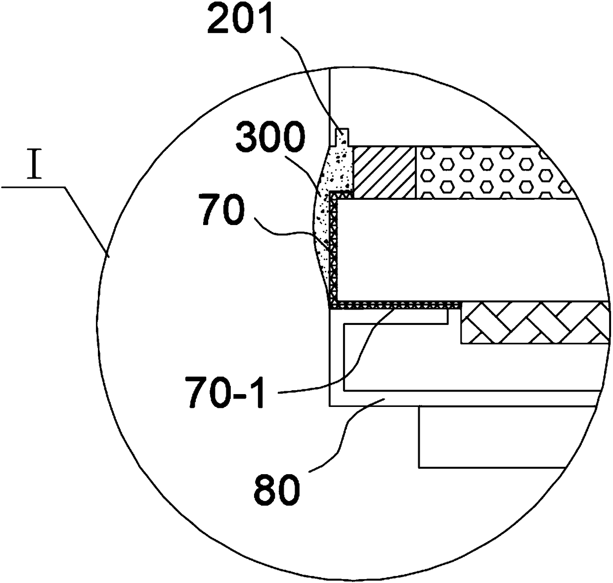
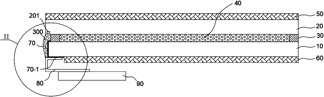
[0021] see figure 1 and image 3 , the liquid crystal panel of the present invention includes a TFT (Thin Film Transistor, thin film transistor) substrate 10 opposite to the backlight assembly, a sealant 30 disposed on the upper surface of the TFT substrate 10 and a CF (Color filter) cover disposed on the sealant 30 , color filter) substrate 20, the sealant 30 between the TFT substrate 10 and the CF substrate 20 is provided with a liquid crystal 40, it can be understood that the area where the liquid crystal 40 is provided forms the display area of ​​the liquid crystal panel, wherein the TFT su...


PUM


Abstract

The invention discloses a liquid crystal display panel which comprises a TFT (thin film transistor) substrate, frame sealing rubber, a CF (color filter) substrate, liquid crystals and a lead out line.The frame sealing rubber is arranged at the edge of the upper surface of the TFT substrate in an enclosed manner, the CF substrate is arranged on the frame sealing rubber in a covering manner, the liquid crystals are injected into the inner side of the frame sealing rubber, the end surface of the same side of the TFT substrate and the CF substrate exceeds the end surface of the corresponding sideof the frame sealing rubber, one end of the lead out line is connected with an electrode wire of the upper surface of an exceeding portion of the TFT substrate, and the other end of the lead out lineis bent and led out to the back surface of the TFT substrate to form a binding terminal. The invention further discloses a display device. According to the liquid crystal display panel, the CF substrate and an upper polarizer of the CF substrate serve as viewing surfaces, printing of TFT side circuits is omitted, cost is reduced, the binding terminal of the liquid crystal display panel is arranged on the back surface of the TFT substrate through the lead out line, the CF substrate above an exceeding end of the front surface of the TFT substrate and the upper polarizer of the CF substrate areincreased, segment gaps of the front surface of the TFT substrate are removed, so that the CF substrate and the upper polarizer of the CF substrate have external observation performance, the width ofa lead area of the front surface can be narrowed, and the screen-to-body ratio of a viewing area is increased.

Description

technical field [0001] The invention relates to the technical field of liquid crystal display, and more specifically, it relates to a liquid crystal panel and a display device. Background technique [0002] The bezel-less (Bezel Less) machine of the liquid crystal display has gradually become a popular design trend. A bezel-less display refers to a display device with an extremely narrow screen frame. Design, one of its advantages is its outstanding appearance. Compared with the monitors with thick borders in the past, borderless can bring a truly horizontal screen, so that the appearance is more fashionable; another advantage is that the use of borderless Displays with bezel technology can well realize display splicing, realizing double screens, triple screens or even multiple screens, while borderless displays can maximize the effect of joint screens. In addition, the borderless display can bring users a wider visual effect, eliminating the sense of restraint of the origi...

Claims


Application Information

Patent Timeline
Patent Type & Authority Applications(China)
IPC IPC(8): G02F1/1345G02F1/1335
CPCG02F1/133514G02F1/13452G02F1/13456G02F1/1339H05K1/028H05K1/119H05K1/147H05K3/285H05K2201/10136H05K2201/10287G02F1/133528G02F1/13458G02F1/1368
Inventor 景小红
Owner HUIZHOU CHINA STAR OPTOELECTRONICS TECHNOLOGY CO LTD
Why Eureka
Try Eureka