
Pixel structure and OLED display panel containing pixel structure

A pixel structure and pixel technology, applied in the field of OLED display panels, can solve the problems of non-full-color display and distortion of display effects, etc.

Pending Publication Date: 2018-05-29
KUNSHAN GO VISIONOX OPTO ELECTRONICS CO LTD
View PDF0 Cites 14 Cited by
  • Summary
  • Abstract
  • Description
  • Claims
  • Application Information

AI Technical Summary

Problems solved by technology

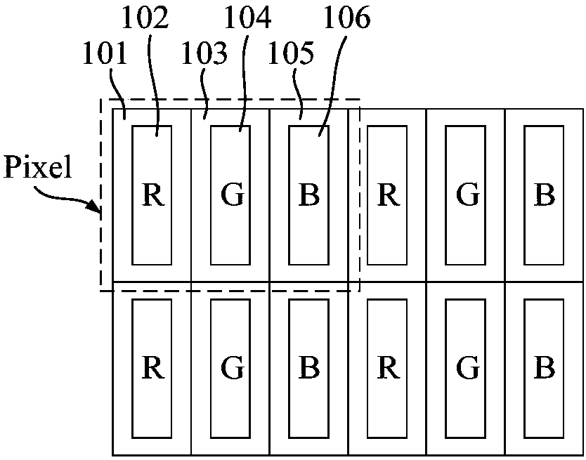
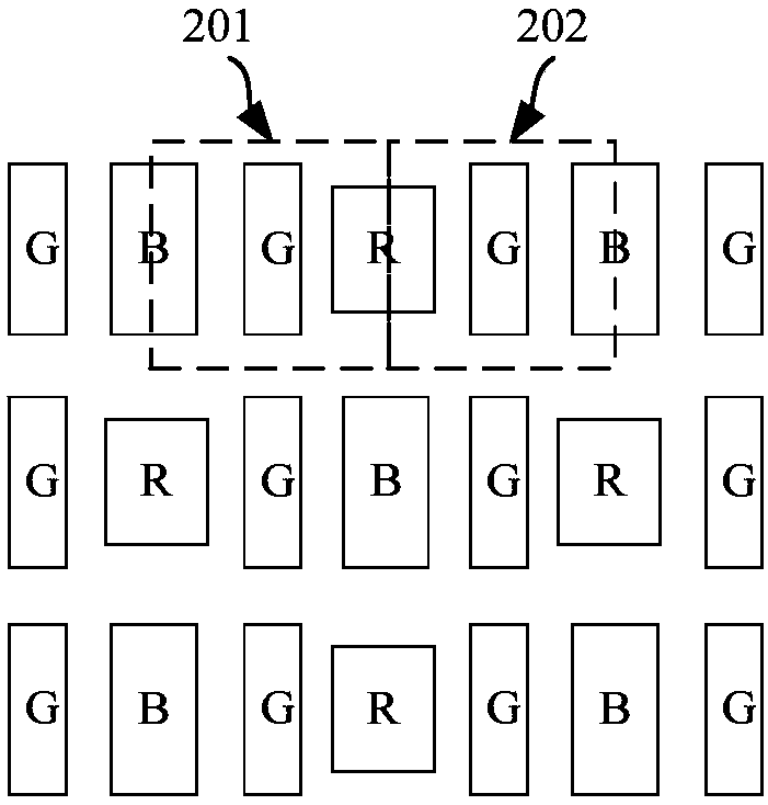
This method can improve the PPI of the display screen. However, in this arrangement, the R and B sub-pixels are shared by adjacent pixel units, and the entire display effect may be distorted, which is not a true full-color display.

Method used


Image

  • Pixel structure and OLED display panel containing pixel structure
  • Pixel structure and OLED display panel containing pixel structure
  • Pixel structure and OLED display panel containing pixel structure

Examples


Embodiment 1

[0030] Figure 4 It is a schematic diagram of pixel arrangement of an OLED display panel in Embodiment 1 of the present invention. Here, the X direction is referred to as the row direction (horizontal direction), and the Y direction is referred to as the column direction (vertical direction). For simplicity, only a part of the OLED display panel is shown in the drawings, and the number of pixels in an actual product is not limited to this, and the number of pixel units can be changed accordingly according to actual display requirements. The first row, the second row, the first column, the second column, etc. mentioned in the present invention are all used to illustrate the present invention and take the reference standard shown in the figure, and do not refer to the rows and columns in the actual product.

[0031] Such as Figure 4 As shown, the pixel structure of the OLED display panel includes a plurality of pixel units arranged in an array, and each pixel unit includes a ...

Embodiment 2

[0040] Figure 5 It is a schematic diagram of the pixel arrangement of the OLED display panel in the second embodiment of the present invention. Such as Figure 5 As shown, each pixel unit includes a first sub-pixel 301, a second sub-pixel 303 and a third sub-pixel 305, the first sub-pixel 301 and the second sub-pixel 303 are arranged in a column, and the third sub-pixel The pixels 305 are arranged in another column, and the arrangement structure of all pixel units in the same row is the same, and the arrangement structure of each pixel unit flipped along the row direction (left and right flipped) is the same as that of the adjacent pixel units in the same column. The cloth structure is the same. For example, the pixel unit (1, 1) in the first row and the first column is flipped 180 degrees along the row direction, and the arrangement structure is the same as the adjacent pixel unit in the same column, that is, the pixel unit (2, 1 in the first column of the second row) ) h...

Embodiment 3

[0043] Figure 6 It is a schematic diagram of pixel arrangement of the OLED display panel in the third embodiment of the present invention. Such as Figure 6As shown, the difference between this embodiment and Embodiment 1 is that the first sub-pixels 301 of all pixel units in the same row are not arranged in a straight line, and at the same time, the second sub-pixels 303 of all pixel units in the same row are not Instead, the first sub-pixels 301 and the second sub-pixels 303 of all pixel units in the same row are alternately arranged on a straight line. For example, the first sub-pixel 301 of the pixel unit (1, 1) in the first row and the first column, the second sub-pixel 303 of the pixel unit (1, 2) in the first row and the second column, the first row and the third column The first sub-pixels 301 of the pixel unit (1, 3) are sequentially arranged on a straight line.


PUM


Abstract

The invention provides a pixel structure and an OLED display panel containing the pixel structure. Each pixel unit comprises a first sub pixel, a second sub pixel and a third sub pixel, wherein the first sub pixel and the second sub pixel are arranged in one column (row), the third sub pixel is arranged in the other column (row), and the total size of the first sub pixel and the second sub pixel along the column (row) direction is larger than the size of the third sub pixel along the column (row) direction. The arrangement structures of the pixel units in the same row (column) are the same. The arrangement structure of each pixel unit after 180-degree turning along the row (column) direction is the same with the arrangement structure of the adjacent pixel unit in the same column (row). Byusing the pixel arrangement mode, the pixel spacing is reduced, the PPI is improved, and the difficulty of the evaporation mask making process and the evaporation process can be lowered.

Description

technical field [0001] The invention relates to the field of display technology, in particular to a pixel structure and an OLED display panel including the pixel structure. Background technique [0002] OLED (Organic Light-Emitting Diode, Organic Light-Emitting Diode) is an active light-emitting device. Compared with the traditional LCD (Liquid Crystal Display, liquid crystal display) display method, the OLED display technology does not require a backlight and has the characteristic of self-luminescence. OLED uses a thin film of organic material and a glass substrate. When an electric current passes through it, the organic material will emit light. Therefore, OLED display panels can significantly save power, can be made lighter and thinner, can withstand a wider range of temperature changes than LCD display panels, and have a larger viewing angle. OLED display panel is expected to become the next-generation flat panel display technology after LCD, and it is one of the most...

Claims


Application Information

Patent Timeline
IPC IPC(8): H01L27/32
CPCH10K59/121
Inventor 余珺胡小叙曹朝干常建兵韩珍珍朱修剑
Owner KUNSHAN GO VISIONOX OPTO ELECTRONICS CO LTD
Learn More