
An automatic shaping and cutting device for a chip carrier

A chip carrier, automatic technology, applied in the field of electronic information, can solve the problems of long production cycle, low production efficiency, low degree of automation, etc., to prevent deformation and ensure the effect of cutting effect

Active Publication Date: 2019-12-31
江苏恩微电子有限公司
View PDF6 Cites 0 Cited by
  • Summary
  • Abstract
  • Description
  • Claims
  • Application Information

AI Technical Summary

Problems solved by technology

At present, the production and processing technology of the basic carrier of plastic chips in the factory is relatively mature, but the cost of most of the stereotyped cutting equipment is relatively high. Due to cost constraints, most of the equipment used by small and medium factories has a low degree of automation and low production efficiency. longer period

Method used


Image

  • An automatic shaping and cutting device for a chip carrier
  • An automatic shaping and cutting device for a chip carrier
  • An automatic shaping and cutting device for a chip carrier

Examples


Embodiment Construction

[0029] The following will clearly and completely describe the technical solutions in the embodiments of the present invention with reference to the accompanying drawings in the embodiments of the present invention. Obviously, the described embodiments are only some, not all, embodiments of the present invention. Based on the embodiments of the present invention, all other embodiments obtained by persons of ordinary skill in the art without making creative efforts belong to the protection scope of the present invention.

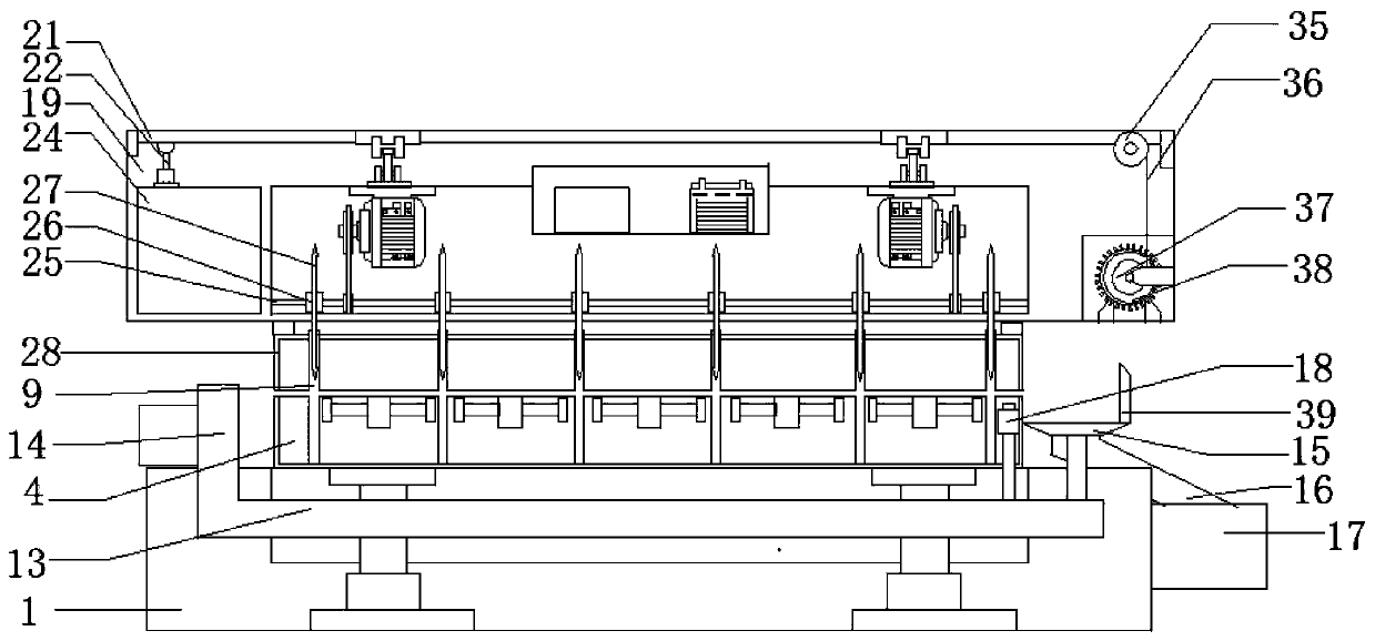
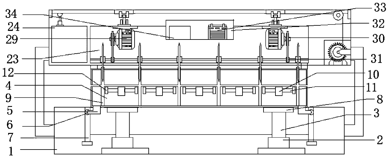
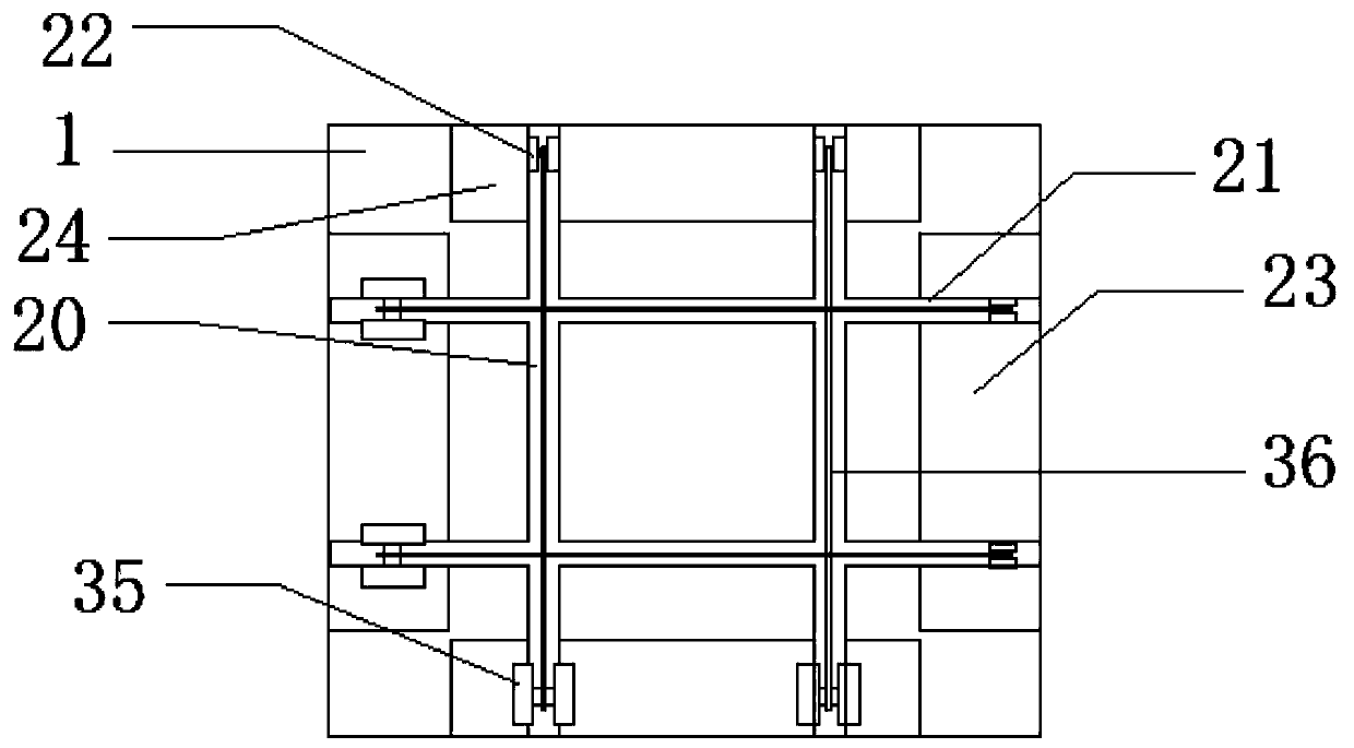
[0030]see Figure 1-7 , the present invention provides a technical solution: an automatic sizing and cutting device for a chip carrier, including a bottom support box 1, the bottom inner walls of both sides of the bottom support box 1 are fixedly connected with a first cylinder 2 through a supporter, and the second The top of a cylinder 2 is fixedly connected with the first air pressure telescopic rod 3, the top of the bottom support box 1 is provided with a g...


PUM


Abstract

The invention discloses an automatic shaping and cutting device for chip carriers and relates to the technical field of electronic information. The automatic shaping and cutting device for the chip carriers comprises a bottom end supporting box, wherein the inner walls of the bottom ends of the two sides of the bottom end supporting box are fixedly connected with first air cylinders through supporting devices, the top end of each first air cylinder is fixedly connected with a first air pressure telescopic rod, and the top end of the bottom end supporting box is provided with a groove; the topends of the first air pressure telescopic rods penetrate the outer walls of the top ends of the bottom end supporting box, extend into the groove and are fixedly connected with a carrier bottom end fixing box through second fixators; and the outer walls of the bottom ends of the two sides of the carrier bottom end fixing box are fixedly connected with rotating wheels through first fixators. The automatic shaping and cutting device for the chip carriers mainly aims at plastic chip carriers, and is simple in structure, low in cost and suitable for production and processing of small and medium-sized factories. Meanwhile, the automation degree of the automatic shaping and cutting device is high, the production efficiency of the plastic chip carriers is greatly improved, and the production cycle is shortened.

Description

technical field [0001] The invention relates to the technical field of electronic information, in particular to an automatic shaping and cutting device for a chip carrier. Background technique [0002] Chip carrier is a basic packaging form of surface mount integrated circuits. It encapsulates integrated circuit chips and inner leads in plastic or ceramic shells, and leads corresponding soldering terminals or short leads to the four sides of the shell. At present, the production and processing technology of the basic carrier of plastic chips in the factory is relatively mature, but the cost of most of the stereotyped cutting equipment is relatively high. Due to cost constraints, most of the equipment used by small and medium factories has a low degree of automation and low production efficiency. The cycle is longer. Contents of the invention [0003] A technical problem solved [0004] Aiming at the deficiencies of the prior art, the present invention provides an automat...

Claims


Application Information

Patent Timeline
Patent Type & Authority Patents(China)
IPC IPC(8): B26D11/00B26D1/157B26D5/08B26D5/02B26D7/32B26D7/02B26D7/18
CPCB26D1/157B26D5/02B26D5/08B26D7/02B26D7/18B26D7/32B26D11/00
Inventor 王玉环
Owner 江苏恩微电子有限公司
Learn More