
In-situ integrated additive manufacturing device for nano-metal circuit

A nano-metal, additive manufacturing technology, applied in additive processing, printed circuit components, three-dimensional rigid printed circuit boards, etc., can solve problems such as low efficiency, long preparation time, and inability to freely design and manufacture electronic circuits. To achieve the effect of improving flexibility, improving density and preventing oxidation

Active Publication Date: 2018-06-01
HARBIN INST OF TECH AT WEIHAI
View PDF6 Cites 2 Cited by
  • Summary
  • Abstract
  • Description
  • Claims
  • Application Information

AI Technical Summary

Problems solved by technology

The preparation time is long, the efficiency is low, and the size of the sintered product is also limited by the size of the sintering furnace
In addition to the above problems, many electronic circuit printings are still essentially two-dimensional plane printing, which cannot meet the needs of free design and manufacture of electronic circuits on complex three-dimensional curved surfaces.

Method used


Image

  • In-situ integrated additive manufacturing device for nano-metal circuit
  • In-situ integrated additive manufacturing device for nano-metal circuit

Examples


Embodiment Construction

[0024] The present invention will be further described below in conjunction with the accompanying drawings.

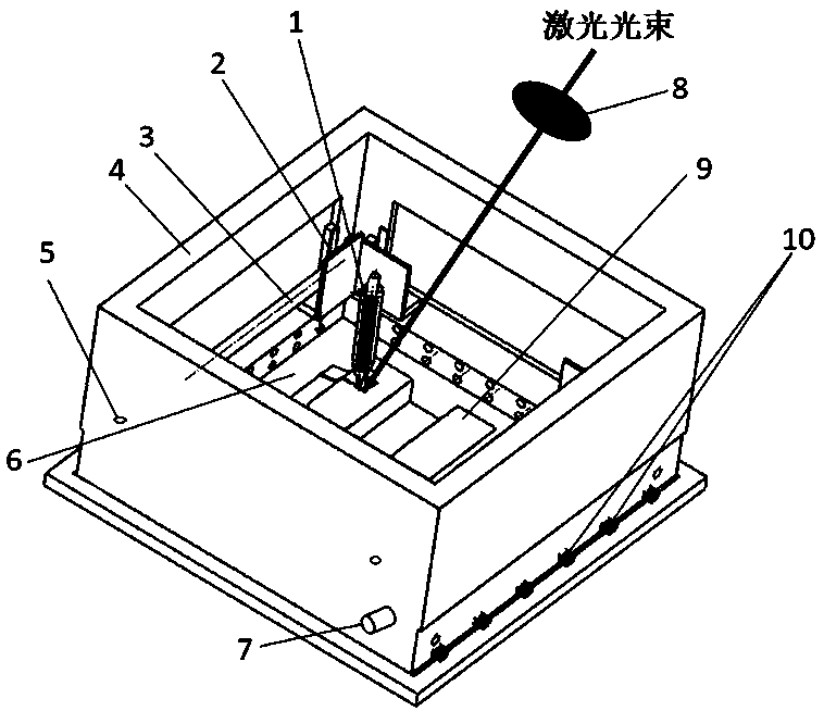
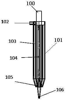
[0025] An in-situ integrated additive manufacturing device for nanometer metal circuits, comprising: a forming chamber 4, an additive feeding module 1, an in-situ irradiation reduction module, an in-situ sintering module, an in-situ heating module, and a gas protection module, wherein the forming chamber The bottom of 4 is provided with an in-situ heating module. The in-situ heating module includes a heating base plate 6 arranged at the bottom of the forming chamber. The heating base plate 6 is heated by a built-in resistance wire, and the temperature is displayed and controlled by a thermocouple, and the upper surface of the heating base plate 6 is heated. The processing platform used to place the parts to be processed, the heating bottom plate 6 described in this embodiment is fixed on the bottom of the forming chamber 4 by four adjustable spring screws, and can be le...


PUM


Abstract

The invention discloses an in-situ integrated additive manufacturing device for a nano-metal circuit, and the device employs a modular design, achieves the high integration of an additive delivery module of nano-metal, in-situ heating, in-situ laser sintering, in-situ irradiation reduction and gas protection, and achieves the coordinative control. The device can achieve the preparation of a two-dimensional plane circuit, and also can achieve the preparation of a three-dimensional circuit which is complex in complex surface curvature and curvature changes. According to the invention, the forming, in-situ reduction and in-situ sintering of a nano-metal circuit are integrated, thereby solving a problem nano-metal oxidation, and improving the efficiency. The manufacturing shape and size are not limited by a sintering furnace, thereby enlarging the application range of an additive manufacturing method, solving a problem of non-uniform distribution metal particles in a preparation process ofa conventional nano-metall circuit or residual gaps after sintering, improving the circuit compactness and consistency, and finally obtaining a circuit with the good performances.

Description

technical field [0001] The invention belongs to the technical field of printed electronics, and mainly relates to an in-situ integrated additive manufacturing device for nanometer metal circuits. Background technique [0002] Metal wiring or electronic circuit manufacturing is very important in the electronics industry. In traditional printed circuits, photolithography is mostly used. As a "subtractive material" manufacturing technology, this technology has problems such as environmental pollution, waste of raw materials, many processes, low efficiency and yield. For the manufacture of complex electronic circuits, especially three-dimensional circuits, this technology has certain limitations. As a new manufacturing technology, additive manufacturing technology can effectively solve the above problems. As one of the important materials for additive manufacturing, nano-metal materials, especially nano-metal conductive ink / paste, have also received extensive attention and re...

Claims


Application Information

Patent Timeline
IPC IPC(8): H05K1/02B33Y30/00
CPCB33Y30/00H05K1/0284
Inventor 刘淑杰李宇杰王喆赵云桐刘长林霍曜
Owner HARBIN INST OF TECH AT WEIHAI
Learn More