
Semiconductor device and method of forming the same

A semiconductor and device technology, applied in the field of semiconductor devices and their formation, can solve the problems of poor overall performance of semiconductor devices, achieve the effects of reduced on-state current, high threshold voltage, and increased beta ratio

Active Publication Date: 2019-09-27
SEMICON MFG INT (SHANGHAI) CORP +1
View PDF5 Cites 0 Cited by
  • Summary
  • Abstract
  • Description
  • Claims
  • Application Information

AI Technical Summary

Problems solved by technology

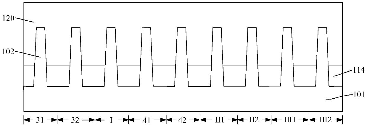
[0004] However, the performance of the static random access memory in the semiconductor device formed by the prior art needs to be further improved, so that the overall performance of the semiconductor device is relatively poor

Method used


Image

  • Semiconductor device and method of forming the same
  • Semiconductor device and method of forming the same
  • Semiconductor device and method of forming the same

Examples


Embodiment Construction

[0012] It can be seen from the background art that the performance of the SRAM in the semiconductor device formed in the prior art needs to be improved.

[0013] For the SRAM, it mainly includes a pull-up (PU, Pull Up) transistor, a pull-down (PD, PullDown) transistor and a pass gate (PG, Pass Gate) transistor. The read margin of the memory plays a key role in the performance of the memory. If the read margin performance of the memory can be improved, the yield rate of the memory will be improved, and the overall performance of the semiconductor device will be improved accordingly.

[0014] Research has found that the read redundancy of the memory is directly proportional to the beta ratio, and the beta ratio is the ratio between the on-state current of the pull-down transistor and the on-state current of the channel gate transistor.

[0015] For a memory cell in a memory with a 122 structure, the memory cell has one pull-up transistor, two pull-down transistors, and two pass-...


PUM


Abstract

A semiconductor device and a forming method thereof, the forming method comprising: forming a gate dielectric layer; forming a first work function layer on the gate dielectric layer; forming a second work function layer on the first work function layer; removing the second P-type threshold Voltage region, the second N-type threshold voltage region and the second work function layer of the first pull-down transistor region; remove the second N-type threshold voltage region and the first work function layer of the first pull-down transistor region; in the remaining second A third work function layer is formed on the work function layer, on the first work function layer of the second P-type threshold voltage region, on the gate dielectric layer of the second N-type threshold voltage region and the first pull-down transistor region, and the third work function layer The thickness of the layer is less than the thickness of the first work function layer; remove the first N-type threshold voltage region, the second pull-down transistor region, the third work function layer and the second work function layer of the channel gate transistor region; A fourth work function layer is formed on the function layer and the third work function layer. The present invention improves read redundancy of semiconductor devices.

Description

technical field [0001] The invention relates to the technical field of semiconductor manufacturing, in particular to a semiconductor device and a forming method thereof. Background technique [0002] In the current semiconductor industry, integrated circuit products can be mainly divided into three types: logic, memory and analog circuits, among which memory devices account for a considerable proportion of integrated circuit products. With the development of semiconductor technology, storage devices are more widely used, and the storage device and other device regions need to be formed on a chip at the same time to form an embedded semiconductor storage device. For example, to embed the storage device in the central processing unit, it is necessary to make the storage device compatible with the embedded central processing unit platform, and maintain the specifications and corresponding electrical performance of the original storage device. [0003] Generally, the memory dev...

Claims


Application Information

Patent Timeline
Patent Type & Authority Patents(China)
IPC IPC(8): H01L27/11
CPCH10B10/18H10B10/00H10B10/12H01L27/092H01L21/823821H01L21/823842H01L27/0924H01L29/4958H01L29/4966H01L29/66545H01L21/28079H01L21/28088H01L21/82385H01L21/823857H01L27/0922H01L29/42372
Inventor 李勇
Owner SEMICON MFG INT (SHANGHAI) CORP
Learn More