Pixel circuit, driving method thereof and display device

A pixel circuit and capacitor technology, applied in static indicators, instruments, etc., can solve the problems of uneven display and unstable grid voltage of display devices, and achieve stable current, grid voltage, and uniformity. Effect

Inactive Publication Date: 2018-06-19
KUNSHAN GO VISIONOX OPTO ELECTRONICS CO LTD
View PDF4 Cites 10 Cited by
  • Summary
  • Abstract
  • Description
  • Claims
  • Application Information

AI Technical Summary

Problems solved by technology

[0005] The embodiment of the present application provides a pixel circuit, its driving method, and a display device, which are used to solve the problem of uneven display in the display device due to the instability of the gate voltage of the driving thin film transistor in the pixel circuit in the existing display device.

Method used


Image

  • Pixel circuit, driving method thereof and display device
  • Pixel circuit, driving method thereof and display device
  • Pixel circuit, driving method thereof and display device

Examples


Embodiment 1

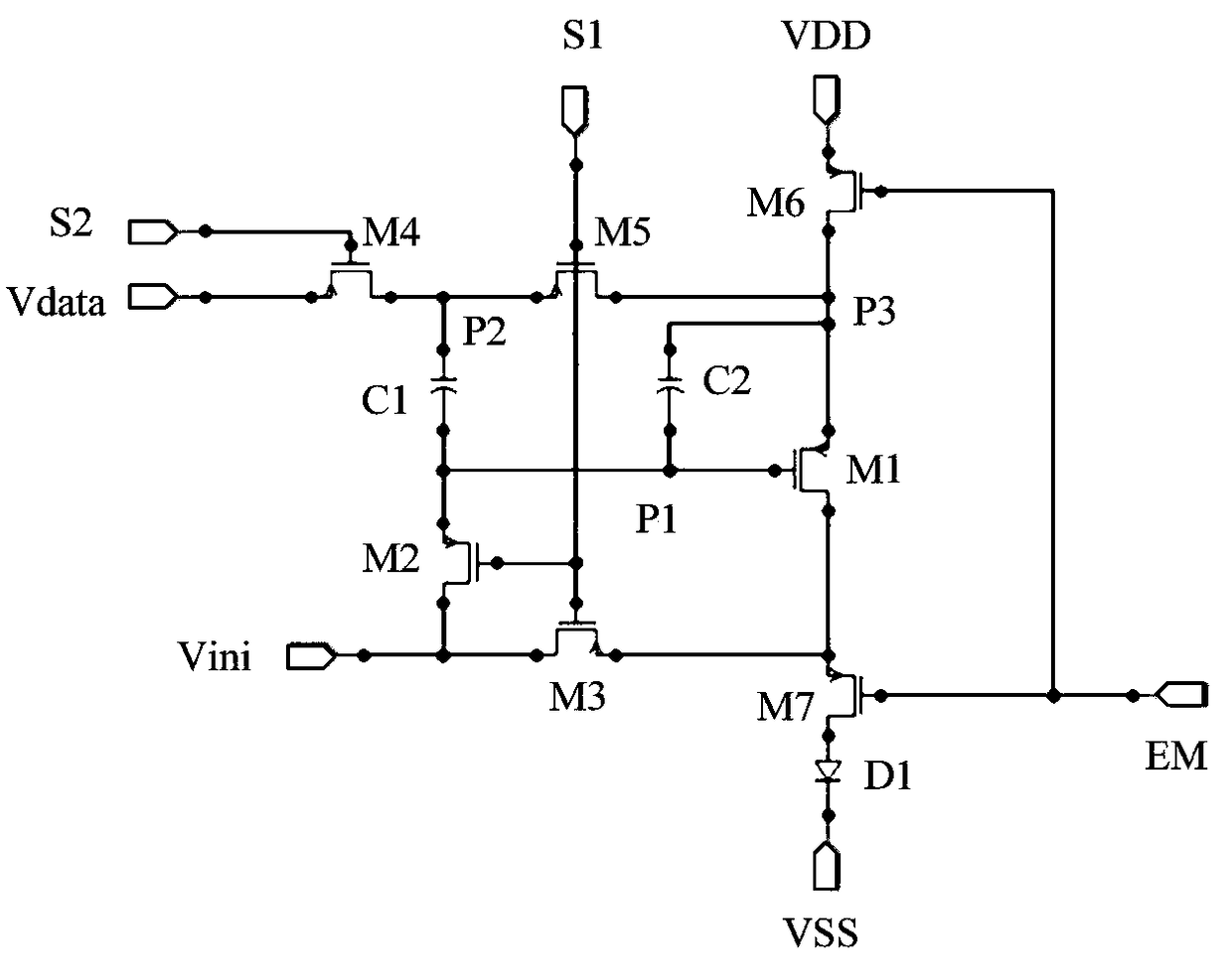
[0043] figure 1 A schematic structural diagram of a pixel circuit provided in an embodiment of the present application. The pixel circuit is as follows.

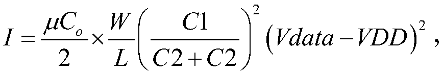
[0044] Such as figure 1 As shown, the pixel circuit includes a first thin film transistor M1, a second thin film transistor M2, a third thin film transistor M3, a fourth thin film transistor M4, a fifth thin film transistor M5, a sixth thin film transistor M6, a seventh thin film transistor M7, The first capacitor C1, the second capacitor C2 and the light emitting diode D1.

[0045] in, figure 1 In the pixel circuit shown, the first thin film transistor M1, the second thin film transistor M2, the third thin film transistor M3, the fourth thin film transistor M4, the fifth thin film transistor M5, the sixth thin film transistor M6 and the seventh thin film transistor M7 are all P-type thin film transistor, light emitting diode D1 is OLED.

[0046] figure 1 The circuit connection structure of the pixel circuit shown is a...

Embodiment 2

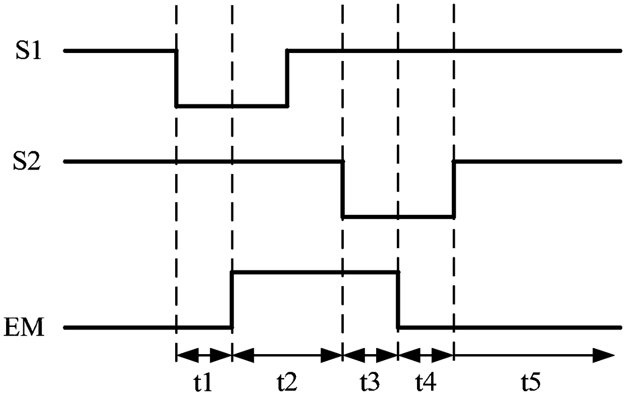
[0071] figure 2 A timing diagram of a pixel circuit driving method provided in an embodiment of the present application, the pixel circuit driving method corresponding to the timing diagram can be used to drive figure 1 The pixel circuit shown.

[0072] figure 2 The driving method of the pixel circuit corresponding to the timing diagram shown may include five stages: the first stage t1, the second stage t2, the third stage t3, the fourth stage t4 and the fifth stage t5, wherein, S1 may be figure 1 The first scanning signal provided by the first scanning line described in the illustrated embodiment, S2 may be figure 1 The second scanning signal provided by the second scanning line described in the illustrated embodiment, EM may be figure 1 The light emission control signal provided by the light emission control line described in the illustrated embodiment.

[0073] figure 2 The driving method of the pixel circuit corresponding to the timing diagram shown specifically in...

Embodiment 3

[0116] An embodiment of the present application further provides a display device, which may include the pixel circuit described in Embodiment 1.


PUM


Abstract

The present invention discloses a pixel circuit, a driving method thereof and a display device. The pixel circuit includes a first thin film transistor, a second thin film transistor, a third thin film transistor, a fourth thin film transistor, a fifth thin film transistor, a sixth thin film transistor, a seventh thin film transistor, a first capacitor, a second capacitor and a light emitting diode. Before the pixel circuit enters a light-emitting phase, a power supply voltage can apply a voltage to a source electrode of a driving thin film transistor, when the pixel circuit enters the light-emitting phase, the power supply voltage can still apply a voltage to a source electrode of the driving thin film transistor, thereby the constant source electrode voltage of the driving thin film transistor can be ensured, so the stable and constant gate voltage of the driving thin film transistor can be ensured under the action of a storage capacitor in the pixel circuit, current which flows through the light-emitting diode is stable and constant, and thus the uniformity of the display of the entire display device is ensured.

Description

technical field [0001] The present application relates to the field of display technology, in particular to a pixel circuit, a driving method thereof, and a display device. Background technique [0002] An organic light-emitting display device is a display device that uses an organic light-emitting diode as a light-emitting device. It has the characteristics of high contrast, thin thickness, wide viewing angle, fast response speed, and low power consumption. It is increasingly used in various display and lighting applications. field. [0003] Generally, a display device may include a plurality of pixels, and the pixel circuit corresponding to each pixel may include a driving thin film transistor and a storage capacitor connected to the gate of the thin film transistor, wherein the storage capacitor can store charges, and In the light-emitting stage of the circuit, the gate voltage of the driving thin film transistor can be controlled to generate a driving current to drive t...

Claims


Application Information

Patent Timeline
Patent Type & Authority Applications(China)
IPC IPC(8): G09G3/3208G09G3/32
CPCG09G3/3208G09G3/32
Inventor 张婷婷黄秀颀张露胡思明韩珍珍朱晖
Owner KUNSHAN GO VISIONOX OPTO ELECTRONICS CO LTD
Why Eureka
Try Eureka