Back lighting type image sensor and formation method thereof

An image sensor and back-illuminated technology, which is applied in the direction of electric solid-state devices, semiconductor devices, electrical components, etc., can solve the problems that the performance of back-illuminated image sensors needs to be improved, so as to save material and process costs, reduce process problems, reduce The effect of power consumption

Inactive Publication Date: 2018-06-19
HUAIAN IMAGING DEVICE MFGR CORP
View PDF5 Cites 2 Cited by
  • Summary
  • Abstract
  • Description
  • Claims
  • Application Information

AI Technical Summary

Problems solved by technology

[0004] However, the performance of existing back-illuminated image sensors needs to be improved

Method used


Image

  • Back lighting type image sensor and formation method thereof
  • Back lighting type image sensor and formation method thereof
  • Back lighting type image sensor and formation method thereof

Examples


Embodiment Construction

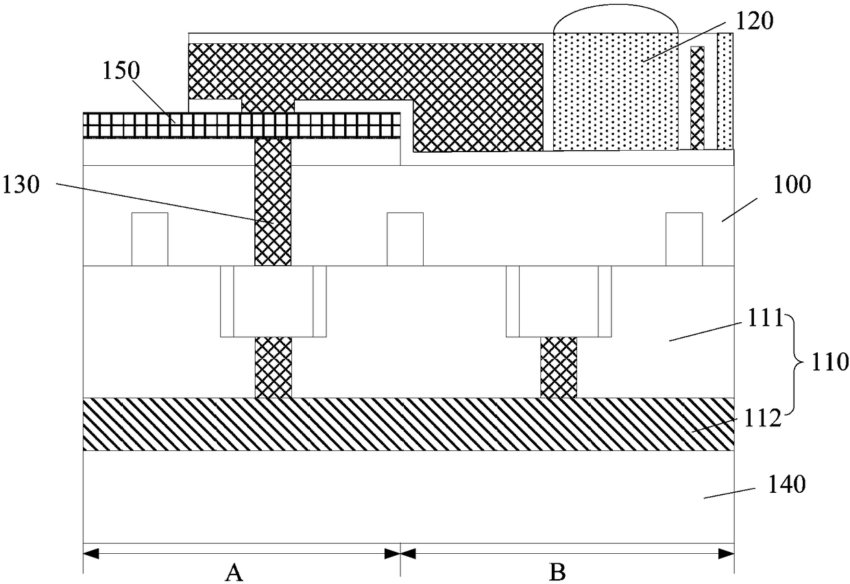
[0021] As mentioned in the background, the performance of back-illuminated image sensors formed by the prior art is relatively poor.

[0022] refer to figure 1 , a structural schematic diagram of a back-illuminated image sensor, including: a backplane substrate 140 and a main body substrate, the main body substrate includes a first region A and a second region B; the main body substrate includes a photosensitive substrate 100, and the photosensitive substrate 100 has an opposite first surface and the second surface, the first surface of the photosensitive substrate 100 has a device layer 110, the device layer 110 has a logic device layer 111 and a metal wire structure 112, the logic device layer 111 is located on the first surface of the photosensitive substrate 100, the metal wire structure 112 and the metal wire structure 112 The carrier substrate 140 is connected, the device layer 110 is connected to the carrier substrate 140, the second surface of the photosensitive substr...


PUM


Abstract

The present invention relates to a back lighting type image sensor and a formation method thereof. The formation method of the back lighting type image sensor comprises the steps of providing a backboard substrate; providing a main body substrate, wherein the main body substrate comprises a first area, a second area, a photoelectric sensing layer and a metal conducting wire structure located on the surface of the photoelectric sensing layer, a photoelectric conversion element is arranged in the photoelectric sensing layer in the second area, the photoelectric sensing layer comprises the relative first and second surfaces, and the metal conducting wire structure is located on the first surface; bonding the metal conducting wire structure and the backboard substrate; then removing the photoelectric sensing layer in the first area from the second surface, exposing the metal conducting wire structure of the first area of the main body substrate, and forming an opening in the photoelectricsensing layer; and then forming a metal grid layer on the second surface of a part of the photoelectric sensing layer of the second area; forming a metal gasket on the surface of the metal conductingwire structure exposed from the opening, and connecting the metal gasket and the metal grid layer; forming a light acceptance structure on the second surface of the photoelectric sensing layer in thesecond area of the main body substrate. The method enables the performance of the back lighting type image sensor to be improved.

Description

technical field [0001] The invention relates to the field of semiconductor manufacturing, in particular to a back-illuminated image sensor and a forming method thereof. Background technique [0002] An image sensor is a semiconductor device that converts light signals into electrical signals. Image sensors are classified into complementary metal oxide (CMOS) image sensors and charge-coupled device (CCD) image sensors. CMOS image sensor has the advantages of simple process, easy integration of other devices, small size, light weight, low power consumption and low cost. Therefore, with the development of image sensing technology, CMOS image sensors are increasingly used in various electronic products instead of CCD image sensors. Currently, CMOS image sensors have been widely used in digital still cameras, digital video cameras, medical imaging devices, automotive imaging devices, and the like. [0003] CMOS image sensors include front illuminated (FSI) image sensors and ba...

Claims


Application Information

Patent Timeline
Patent Type & Authority Applications(China)
IPC IPC(8): H01L27/146
CPCH01L27/14636H01L27/1464H01L27/14643H01L27/14689
Inventor 吴明吴孝哲林宗贤吴龙江薛超朱晓彤
Owner HUAIAN IMAGING DEVICE MFGR CORP
Why Eureka
Try Eureka