A method and device for testing recombination current density at a metal-semiconductor interface

A metal semiconductor, current density technology, applied in the direction of current density measurement, etc., can solve the problems of inaccurate test results, low accuracy, and damage to the surface state of non-metallic areas

Active Publication Date: 2020-04-14
CSI SOLAR TECH (JIAXING) CO LTD
View PDF4 Cites 3 Cited by
  • Summary
  • Abstract
  • Description
  • Claims
  • Application Information

AI Technical Summary

Problems solved by technology

[0004] Since no metal can appear during the QSSPC test, the existing test method needs to corrode the sintered metal in the sample to be tested first, and the corrosion process will destroy the surface state of the non-metallic area
The corroded metal needs to be completely cleaned, and QSSPC has high requirements on the cleanliness of the cleaning, otherwise the test results will be inaccurate or the test data will not be available.
Moreover, since the metal will be corroded during the QSSPC test, the measured metal interface recombination current density is the interface recombination current density after corroding the metal, that is, the measured result is an equivalent value, not the real recombination current density of the metal interface
[0005] The composite current density test method of the metal interface in the prior art is complicated to operate, requires high cleaning and cleanliness, and the test results fluctuate greatly and the accuracy is not high

Method used


Image

  • A method and device for testing recombination current density at a metal-semiconductor interface
  • A method and device for testing recombination current density at a metal-semiconductor interface
  • A method and device for testing recombination current density at a metal-semiconductor interface

Examples


Embodiment 1

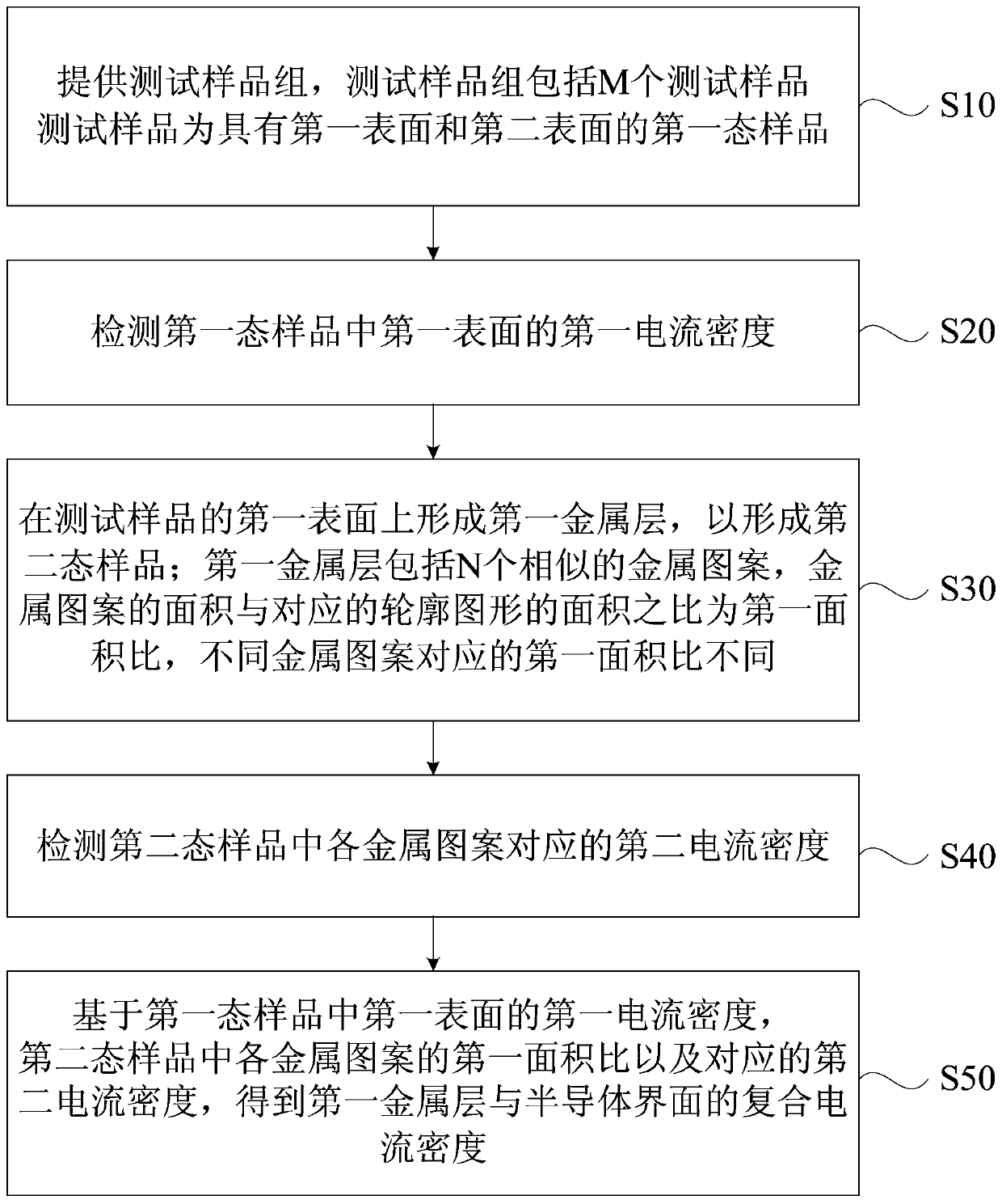
[0036] figure 1 It is a flowchart of a test method for recombination current density at a metal-semiconductor interface provided by Embodiment 1 of the present invention. see figure 1 , an embodiment of the present invention provides a method for testing the recombination current density at a metal-semiconductor interface, including:

[0037] S10. Provide a test sample group, the test sample group includes M test samples, the test sample is a first-state sample having a first surface and a second surface, wherein the test sample is a semiconductor sample, and the first One surface is the side where the N region is located in the P-type substrate, and the second surface is the side where the P region is located in the P-type substrate; or, the first surface is the side where the P region is located in the N-type substrate, The second surface is the side of the N-type substrate where the N region is located.

[0038] Wherein, the test sample is a semiconductor sample, includi...

Embodiment 2

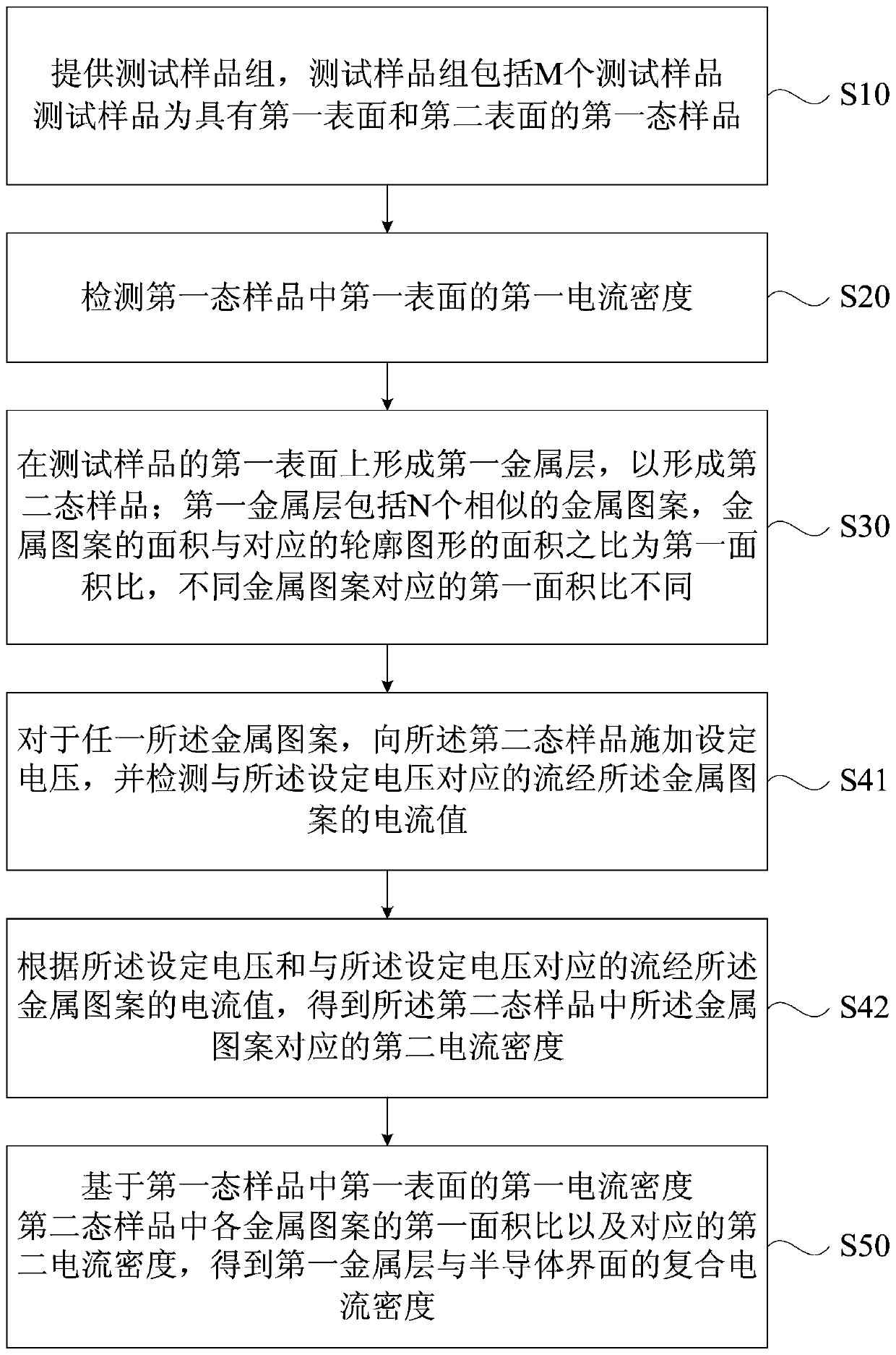
[0063] image 3 It is a flow chart of a test method for recombination current density at a metal-semiconductor interface provided by Embodiment 2 of the present invention. This embodiment is a specific example of the first embodiment. For example, see image 3 , the metal-semiconductor interface recombination current density test method includes:

[0064] S10. Provide a test sample group, the test sample group includes M test samples, the test sample is a first-state sample having a first surface and a second surface, wherein the test sample is a semiconductor sample, and the first One surface is the side where the N-region in the P-type substrate is located or the side where the P-region is located in the N-type substrate, and the second surface is the side where the P-region is located in the P-type substrate or the side where the N-region is located in the N-type substrate side.

[0065] S20. Detect a first current density on the first surface in the first state sample....

Embodiment 3

[0092] Figure 5 It is a schematic structural diagram of a current density testing device provided in Embodiment 3 of the present invention. In the method for testing the recombination current density at the metal-semiconductor interface in the above embodiment, the current density testing device is used to detect the second current density corresponding to each of the metal patterns in the second-state sample. see Figure 5 , the current density test device includes a test platform 1, a flat plate electrode 2, a test probe 3, a current tester 4, a voltage tester 5 and a current and voltage source 6.

[0093] continue to see Figure 5 , the test platform 1 is used to place the test sample 10; the flat electrode 2 is opposite to the test platform 1, and the flat electrode 2 is separated from the test platform 1 by a set distance to form a test area for accommodating the test sample 10; the flat electrode 2 is set There is a through hole through the plate electrode 2; the tes...


PUM


Abstract

The invention discloses a method and device for testing metal semiconductor interface recombination current density. The method includes: providing a testing sample group, wherein each testing sampleis a first-state sample with a first surface and a second surface; detecting the first current density of the first surface of each first-state sample; forming a first metal layer on each first surface to form a second-state sample; each first metal layer comprises N similar metal patterns, and the first area ratios corresponding to different metal patterns are different; detecting second currentdensity corresponding to each metal pattern in each second-state sample; acquiring the recombination current density of each first metal layer and a semiconductor interface according to the corresponding first current density, the first area ratio of each metal pattern and the corresponding second current density. The method and device has the advantages that the metal semiconductor interface recombination current density can be tested simply and fast, and the testing result is real and accurate.

Description

technical field [0001] Embodiments of the present invention relate to current density testing technology, and in particular to a testing method and current density testing device for recombination current density at a metal-semiconductor interface. Background technique [0002] The recombination current density between metal and semiconductor interfaces has important applications in many fields. For example, the recombination of carriers in a solar cell is one of the most important factors affecting the efficiency of a solar cell, and the recombination at the metal-semiconductor interface occupies an important proportion. Accurate and convenient testing of the recombination current density at the metal-semiconductor interface plays an important role in improving battery design and optimizing process technology. [0003] At this stage, the metal paste separating the parallel line patterns is printed on the semiconductor material and sintered to form the sample to be tested. ...

Claims


Application Information

Patent Timeline
Patent Type & Authority Patents(China)
IPC IPC(8): G01R19/08
CPCG01R19/08
Inventor 万松博邓伟伟蒋方丹邢国强
Owner CSI SOLAR TECH (JIAXING) CO LTD
Why Eureka
Try Eureka