Display substrate, display panel and manufacture method thereof

A technology for a display substrate and a manufacturing method, which is applied to identification devices, nonlinear optics, instruments, etc., can solve problems such as product defects, and achieve the effects of not affecting production capacity, improving product yield, and reducing micro-damage

Inactive Publication Date: 2018-06-22
BOE TECH GRP CO LTD +1
View PDF9 Cites 4 Cited by
  • Summary
  • Abstract
  • Description
  • Claims
  • Application Information

AI Technical Summary

Problems solved by technology

[0004] In view of this, the present invention provides a display substrate, a display panel and a manufacturing method thereof, which are used to solve the problem of defective products caused by static electricity in the process of the existing display substrate

Method used


Image

  • Display substrate, display panel and manufacture method thereof
  • Display substrate, display panel and manufacture method thereof
  • Display substrate, display panel and manufacture method thereof

Examples


Embodiment Construction

[0031] In order to make the purpose, technical solutions and advantages of the embodiments of the present invention more clear, the following will clearly and completely describe the technical solutions of the embodiments of the present invention in conjunction with the drawings of the embodiments of the present invention. Apparently, the described embodiments are some, not all, embodiments of the present invention. All other embodiments obtained by those skilled in the art based on the described embodiments of the present invention belong to the protection scope of the present invention.

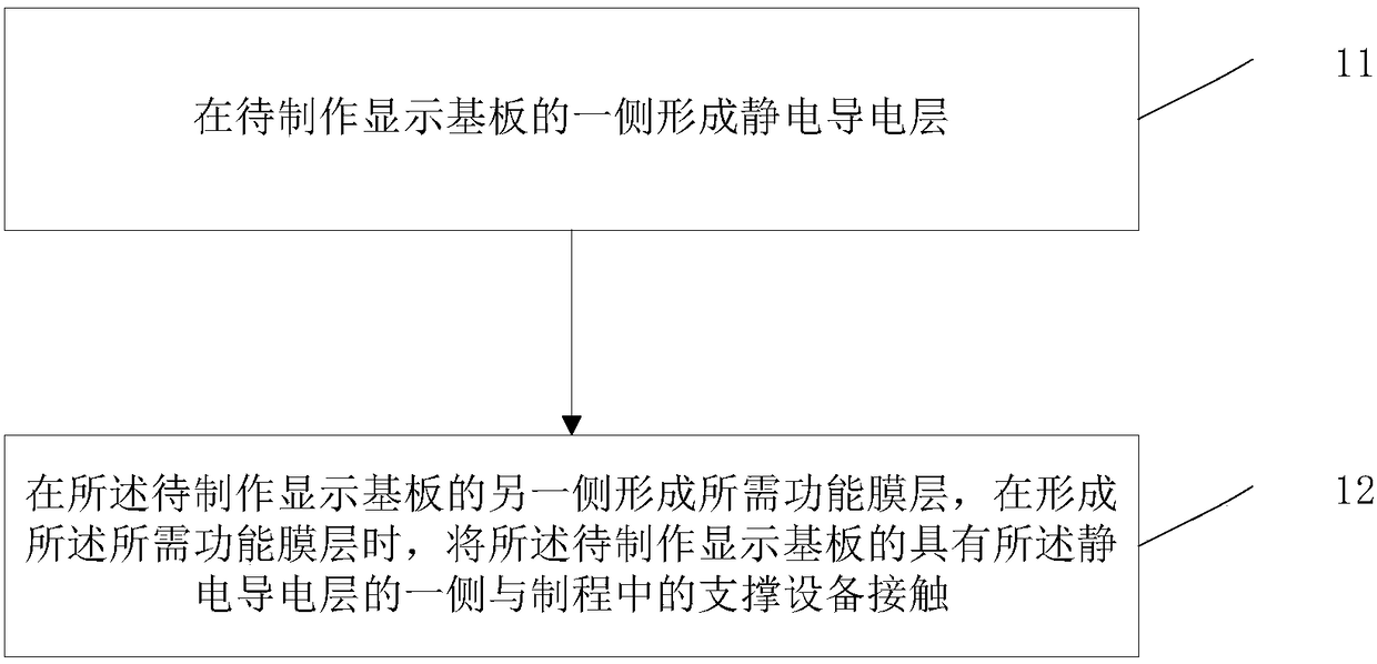
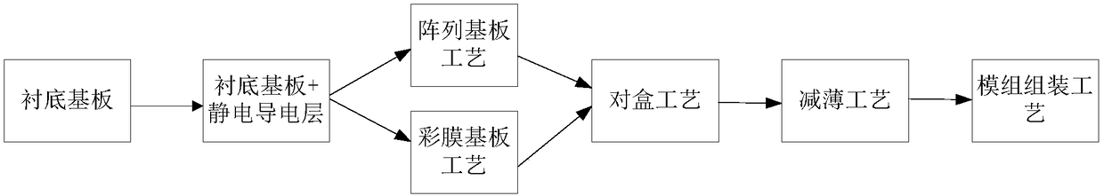
[0032] Please refer to figure 1 , an embodiment of the present invention provides a method for manufacturing a display substrate, including:

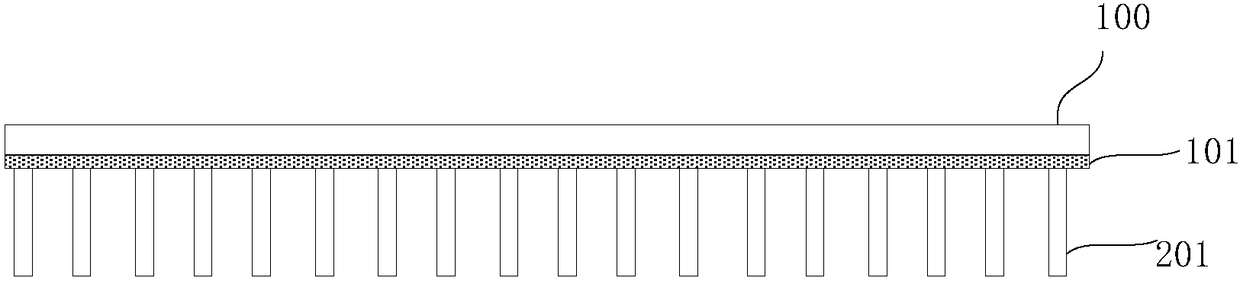
[0033] Step 11: forming an electrostatic conductive layer on one side of the display substrate to be fabricated;

[0034] Step 12: Form a required functional film layer on the other side of the display substrate to be produced, and when forming the...


PUM


Abstract

The invention provides a display substrate, a display panel and a manufacture method thereof. The manufacture method for the display substrate comprises the steps of forming an electrostatic conductive layer on the side of the to-be-manufactured display substrate; forming a desired functional film layer on the other side of the to-be-manufactured display substrate, and conducting contact processing on the side where the electrostatic conductive layer is formed of the to-be-manufactured display substrate and supporting equipment in the manufacture process when the desired functional film layeris formed. The electrostatic conductive layer is a whole layer of the conductive film layer, so that the static electricity on the supporting equipment can be diffused on the entire display substrate,static single point release dose not occur to avoid electrostatic single point breakdown, and the product yield of the display substrate is effectively improved.

Description

technical field [0001] The present invention relates to the field of display technology, in particular to a display substrate, a display panel and a manufacturing method thereof. Background technique [0002] Static electricity can be generated when different substances come into contact, separate or rub against each other. For example, extrusion, cutting, handling, stirring and filtering in the production process, as well as walking, standing up and undressing in life, will generate static electricity, and the electrostatic voltage can reach several thousand volts or even tens of thousands of volts. These static electricity may have little effect on the human body, but for some electrostatic sensitive components, it can directly cause them to lose their normal performance, or even completely lose their normal functions. [0003] In the manufacturing process of the display substrate, due to the cumbersome process steps, the display substrate is often in contact with the sup...

Claims


Application Information

Patent Timeline
Patent Type & Authority Applications(China)
IPC IPC(8): G02F1/1362G02F1/1335G09F9/00
CPCG02F1/133514G02F1/136204G09F9/00
Inventor 石天雷方业周赵艳艳王跃林宋月胜王彦明徐敬义樊祎
Owner BOE TECH GRP CO LTD
Why Eureka
Try Eureka