Pixel circuit, driving method, electroluminescent display panel and display device

A technology of pixel circuits and light-emitting devices, applied in static indicators, instruments, etc., can solve problems such as inconsistent brightness

Active Publication Date: 2018-06-26
BOE TECH GRP CO LTD
View PDF10 Cites 28 Cited by
  • Summary
  • Abstract
  • Description
  • Claims
  • Application Information

AI Technical Summary

Problems solved by technology

[0003] Embodiments of the present invention provide a pixel circuit, a driving method, an electroluminescence display panel, and a display device to solve the problem of inconsistent brightness

Method used


Image

  • Pixel circuit, driving method, electroluminescent display panel and display device
  • Pixel circuit, driving method, electroluminescent display panel and display device
  • Pixel circuit, driving method, electroluminescent display panel and display device

Examples


Embodiment 1

[0132] by Figure 3b Take the pixel circuit shown as an example, and the corresponding input timing diagram is as follows Figure 5a shown. Specifically, the main selection of Figure 5a In the shown input timing diagram, there are three stages in total, namely, the reset stage T1, the data writing stage T2 and the light emitting stage T3.

[0133] In the reset phase T1, Scan1=1, Scan2=0, Scan4=0.

[0134] Since Scan1=1, both the first switch transistor M1 and the third switch transistor M3 are turned on. The turned-on first switch transistor M1 provides the signal of the first reference signal line Vref1 to the second pole D of the driving transistor M0, so as to reset the second pole D of the driving transistor M0 and the light emitting device L, so as to avoid two adjacent poles Luminous interference between display frames. . The turned-on third switch transistor M3 provides the signal of the first reference signal line Vref1 to the gate G of the driving transistor M0...

Embodiment 2

[0143] by Figure 3b Take the pixel circuit shown as an example to illustrate its working process, and the corresponding input timing diagram is as follows Figure 5b shown. Specifically, the main selection of Figure 5b There are four phases in the shown input timing diagram: reset phase T1, threshold compensation phase T2, data writing phase T3 and light emitting phase T4.

[0144] In the reset phase T1, Scan1=1, Scan2=0, Scan4=0.

[0145]Since Scan1=1, both the first switch transistor M1 and the third switch transistor M3 are turned on. The turned-on first switch transistor M1 provides the signal of the first reference signal line Vref1 to the second pole D of the driving transistor M0, so as to reset the second pole D of the driving transistor M0 and the light emitting device L, so as to avoid two adjacent Luminous interference between display frames. The turned-on third switch transistor M3 provides the signal of the first reference signal line Vref1 to the gate G of...

Embodiment 3

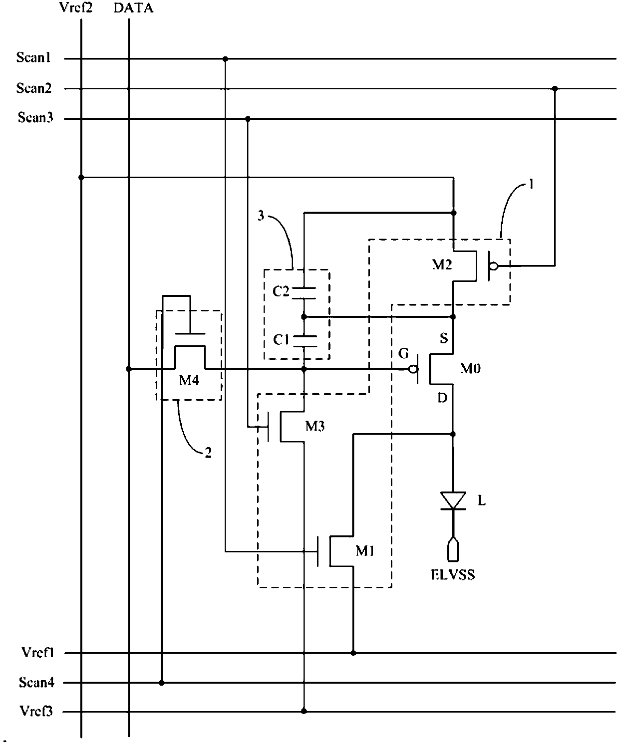
[0154] by Figure 4a Take the pixel circuit shown as an example to illustrate its working process, and the corresponding input timing diagram is as follows Figure 5c shown. Specifically, the main selection of Figure 5c There are four phases in the shown input timing diagram: reset phase T1, threshold compensation phase T2, data writing phase T3 and light emitting phase T4.

[0155] In the reset phase T1, Scan1=1, Scan2=0, Scan3=0, Scan4=0, EM=0.

[0156] Since Scan1=1, the first switching transistor M1 is turned on and provides the signal of the first reference signal line Vref1 to the second pole D of the driving transistor M0 to reset the second pole D of the driving transistor M0 . Since Scan2=0, the second switching transistor M2 is turned on, and the signal of the second reference signal line Vref2 is provided to the first pole S of the driving transistor M0 to reset the first pole S of the driving transistor M0, and through The storage capacitor C1 stores the volta...


PUM


Abstract

The invention discloses a pixel circuit, a driving method, an electroluminescent display panel and a display device. A first pole and a second pole of a driving transistor can be reset in the reset phase by a reset module, and then data signals are written by a data writing module into a grid of the driving transistor, and a driving current is generated by the driving transistor to drive a light emitting device to emit light. In this way, the voltage of the first pole of the driving transistor can be set to a fixed voltage and the voltage of the second pole of the driving transistor can be setto a fixed voltage before each writing of the data signals, so that the influence of the residual voltage of a previous frame on the light emission of the frame can be avoided, and the uniformity oflight emission of the display panel can be improved.

Description

technical field [0001] The invention relates to the field of display technology, in particular to a pixel circuit, a driving method, an electroluminescence display panel and a display device. Background technique [0002] Organic Light Emitting Diode (OLED) is one of the hot spots in the field of flat panel display research today. Compared with Liquid Crystal Display (LCD), OLED display has low energy consumption, low production cost, self-illumination, and wide viewing angle. and quick response. At present, OLED displays have begun to replace traditional LCD displays in display fields such as mobile phones, tablet computers, and digital cameras. Unlike LCDs that use a stable voltage to control brightness, OLEDs are driven by current and require a stable current to control their light emission. Generally, the pixel circuit is set to drive the OLED to emit light. At present, when the pixel circuit drives the OLED to emit light, the voltages of the first electrode and the s...

Claims


Application Information

Patent Timeline
Patent Type & Authority Applications(China)
IPC IPC(8): G09G3/3225
CPCG09G3/3225G09G2300/0852G09G2300/0819G09G2310/0262G09G2300/0861G09G2320/045G09G2320/0233G09G2310/0251G09G3/3233G09G3/3258G09G2310/0278G09G2310/062
Inventor 董甜
Owner BOE TECH GRP CO LTD
Why Eureka
Try Eureka