

A special gold-plated pad manufacturing method
A manufacturing method and pad technology, applied in the reinforcement of conductive patterns, the formation of electrical connections of printed components, the secondary treatment of printed circuits, etc., can solve the problem of board scrapping, corrosion of nickel plating layer, easy to be electroplated with copper or tin, etc. problems, to achieve the effect of quality assurance
- Summary
- Abstract
- Description
- Claims
- Application Information
AI Technical Summary
Problems solved by technology
Method used
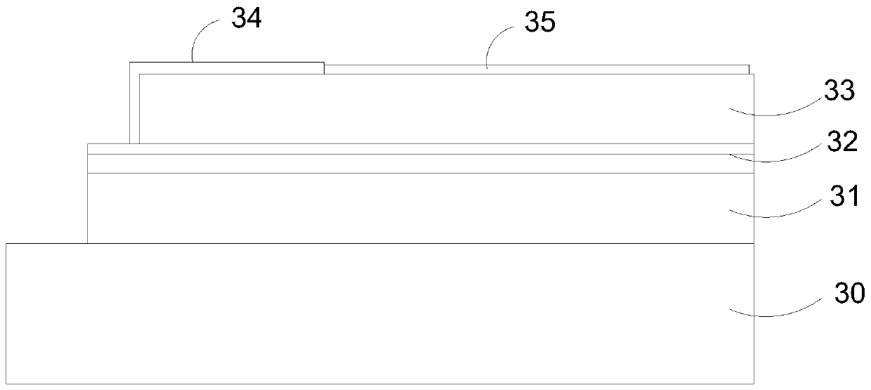
Image

Examples
Embodiment Construction
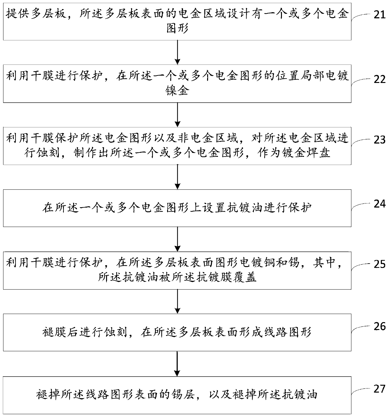
[0021] In order to enable those skilled in the art to better understand the solutions of the present invention, the following will clearly and completely describe the technical solutions in the embodiments of the present invention in conjunction with the drawings in the embodiments of the present invention. Obviously, the described embodiments are only It is an embodiment of a part of the present invention, but not all embodiments. Based on the embodiments of the present invention, all other embodiments obtained by persons of ordinary skill in the art without making creative efforts shall fall within the protection scope of the present invention.
[0022] The terms "first", "second", "third" and the like in the description and claims of the present invention and the above drawings are used to distinguish different objects, rather than to describe a specific order. Furthermore, the terms "include" and "have", as well as any variations thereof, are intended to cover a non-exclus...
PUM
 Abstract
Description
Claims
Application Information