Methods and apparatus for magnetically compensated chip scale atomic clock

An atomic and atomic cavity technology, applied in the field of atomic clocks, which can solve the problems of expensive, difficult to design, and large size of magnetic shields

Active Publication Date: 2018-07-06
TEXAS INSTR INC
View PDF14 Cites 1 Cited by
  • Summary
  • Abstract
  • Description
  • Claims
  • Application Information

AI Technical Summary

Problems solved by technology

Magnetic shields are bulky,...

Method used


Image

  • Methods and apparatus for magnetically compensated chip scale atomic clock
  • Methods and apparatus for magnetically compensated chip scale atomic clock
  • Methods and apparatus for magnetically compensated chip scale atomic clock

Examples


Embodiment Construction

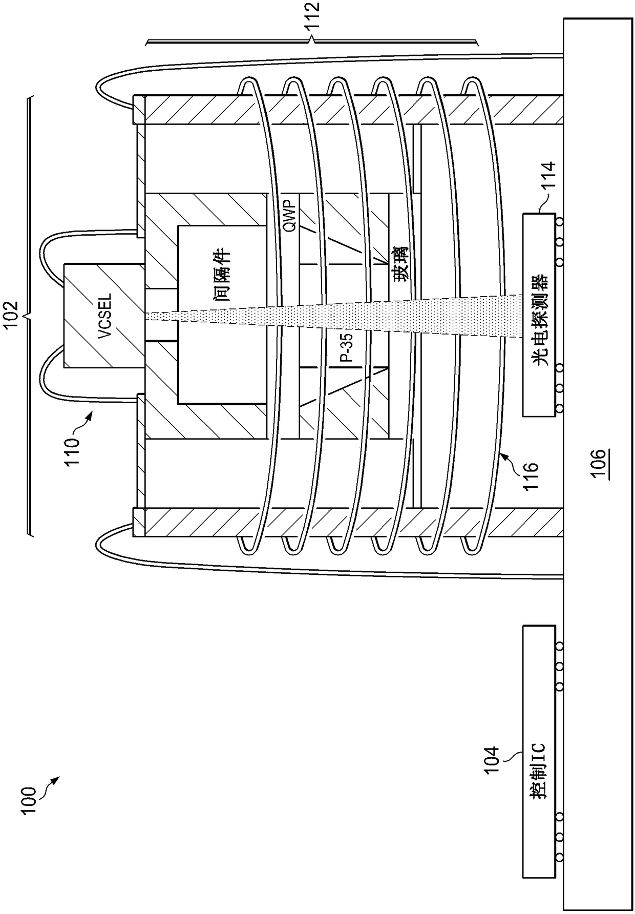
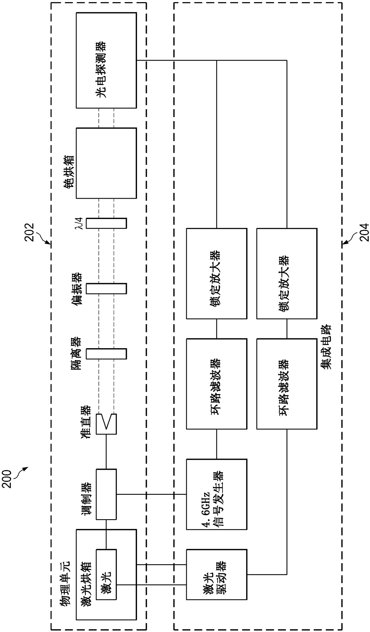
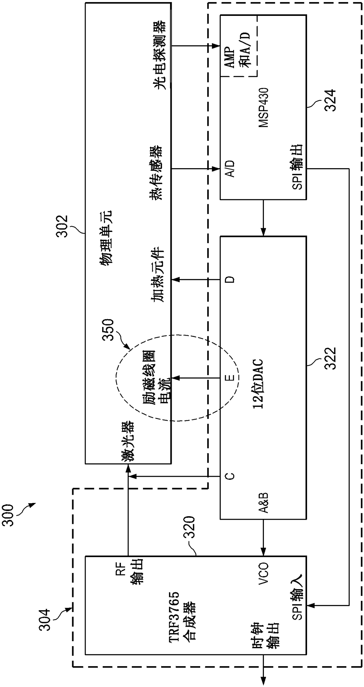
[0012] Corresponding numerals and symbols in the different figures generally refer to corresponding parts unless otherwise indicated. The drawings are not necessarily drawn to scale. The term "coupled" may include connections with intervening elements, and there may be additional elements and various connections between any elements "coupled".

[0013] figure 1 is a cross-sectional view of the chip-scale atomic clock device 100 . In the CSAC device 100 , the physical unit 102 is shown as a component, eg, packaged in a ceramic body and mounted on a packaging substrate 106 . In this example, the physical unit 102 contains a vertical cavity surface emitting laser (VCSEL) 110 with a laser beam directed through a miniature temperature stabilized atomic chamber 112 . The atomic chamber contains a quarter wave polarizer labeled QWP and a chamber labeled P-35 containing a small amount of atomic gas, in this example cesium. The light emission caused by the laser energy striking the...


PUM


Abstract

The application relates to methods and apparatus for magnetically compensated chip scale atomic clock. In described examples, an apparatus includes: a physics cell(302) including: a laser source configured to emit light towards an atomic chamber containing an atomic gas; a photodetector configured to receive emissions from the atomic chamber; and a coil for generating a magnetic field in the atomic chamber; and an electronics circuit(304), including: a controller circuit(324) coupled to the photodetector output and having control outputs to a digital to analog converter circuit(322); the digital to analog converter circuit having a coil current output(E) to adjust the magnetic field, a modulation control output to control a modulation of the light(C), and having an output(A&B) to control avoltage controlled oscillator; and a radio-frequency output circuit(320) having a voltage controlled oscillator coupled to the output of the digital to analog converter circuit and outputting a radiofrequency signal to the laser(LASER) source in the physics cell(302).

Description

technical field [0001] The present application relates generally to atomic clocks, and more particularly to atomic clocks with compensation for fluctuations in external magnetic fields. Background technique [0002] Atomic clocks are very precise and stable timekeeping devices regulated using the natural vibrations of atomic systems. Atomic clock accuracy is increasingly desired in portable navigation systems to improve positional accuracy. Miniature versions of atomic clocks, sometimes called chip-scale atomic clocks (CSACs), use integrated circuits built using advanced semiconductor processes. The stability of the operating environment is a challenge for CSAC devices. An atomic clock can be divided into three parts: the physical part (or physical unit); the electronic part; and the package. These parts can be manufactured separately and assembled later. [0003] The physical units of the CSAC are sometimes constructed using MEMS technology. A typical physical unit has...

Claims


Application Information

Patent Timeline
IPC IPC(8): G04F5/14H03L7/26
CPCG04F5/14H03L7/26H01S5/005H01S5/02438H01S5/02453H01S5/0687H01S5/183H03B17/00G04F5/145
Inventor B·A·克雷默B·S·库克J·A·赫本萨梅尔
Owner TEXAS INSTR INC
Why Eureka
Try Eureka