Device and method for treating micro-stacking structure insulating material surfaces by discharge plasma
A technology of discharge plasma and insulating materials, applied in the direction of insulators, circuits, electrical components, etc., to achieve the effects of improving flashover characteristics along the surface, reducing electric field distortion, and eliminating burrs and protrusions
- Summary
- Abstract
- Description
- Claims
- Application Information
AI Technical Summary
Problems solved by technology
Method used
Image

Examples
Embodiment 1
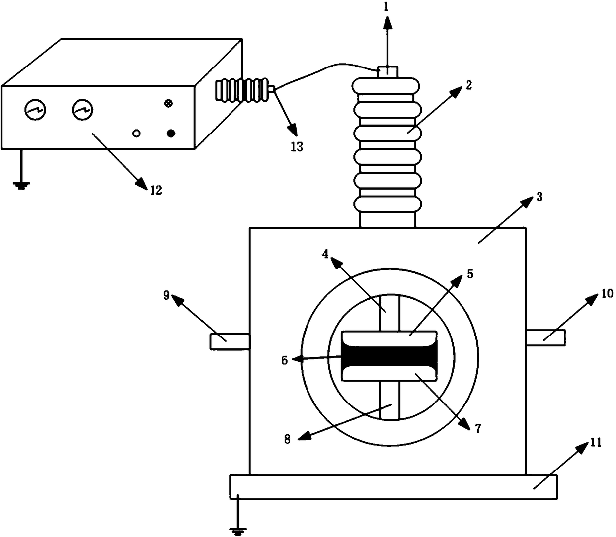
[0034] like figure 2 As shown, what is described in Embodiment 1 of the present invention is a device for treating the surface of an insulating material with a micro-stack structure by a discharge plasma to process a flat-plate-type processed sample, and the device includes:
[0035] A high-voltage lead-in pole 1, one end of which is connected to the pulse power supply 12 through the high-voltage output terminal 13 of the power supply, and the other end of the high-voltage lead-in pole 1 is connected to the high-voltage electrode 5 through the high-voltage conductive rod 4;
[0036] The ground electrode 7 is arranged directly below the high-voltage electrode 5, and the ground electrode 7 is connected to the base 11 through the ground conductive rod 8 and grounded;
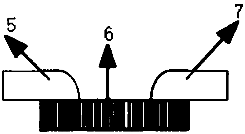
[0037] The processed sample 6 is fixed between the high voltage electrode 5 and the ground electrode 7 , and the processed sample 6 is in close contact with the high voltage electrode 5 and the ground electrode 7 ...
Embodiment 2
[0050] like Figure 5 As shown, what is described in Embodiment 2 of the present invention is a device for treating the surface of a micro-stack structure insulating material with a discharge plasma to process a cylindrical processed sample:
[0051] The difference between this embodiment and Embodiment 1 is that when the sample to be processed is a cylinder or an elliptical cylinder, the high-voltage electrode and the ground electrode are in the shape of a circular plate, and the high-voltage electrode and the The diameter of the ground electrode is more than twice the longest distance between the ground electrode and the contact surface of the processed sample and cannot be less than 20mm. In this embodiment, the low-pressure argon gas is used as the ambient gas, and the processed sample 6 with a diameter of 15 mm and a height of 20 mm is taken as an example for illustration.
[0052] like Figure 5 As shown, the high-voltage lead-in pole 1 of the discharge treatment chamb...
Embodiment 3
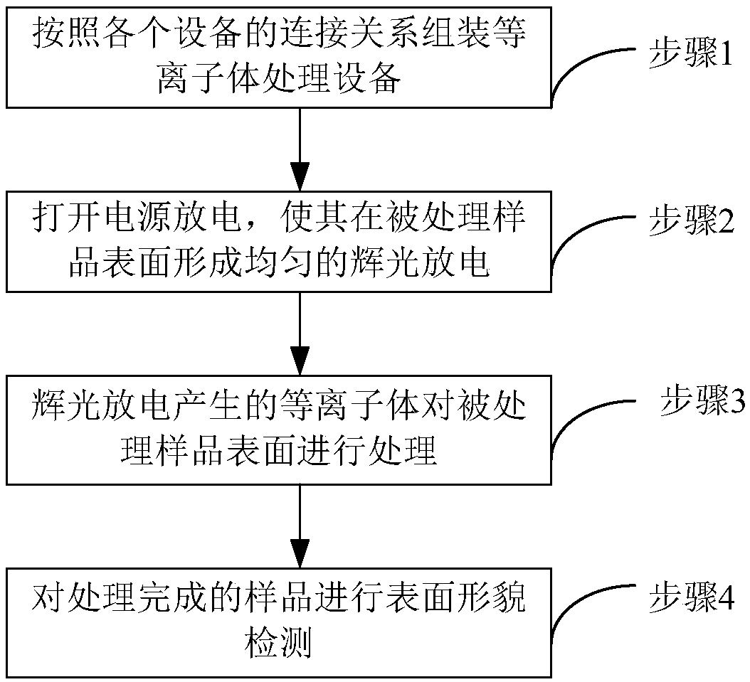
[0056] like figure 1 As shown, what Embodiment 2 of the present invention described is a method for treating the surface of a micro-stack structure insulating material with discharge plasma, the method may further comprise the steps:
[0057] Step 1, according to the connection relationship between each equipment in the discharge plasma treatment micro-stack structure insulating material surface device described in any one of claims 1-9, assemble the device for discharge plasma treatment micro-stack structure insulation material surface The high-voltage lead-in pole 1 of the discharge treatment chamber is fixed on one end of the high-voltage conductive rod 4, and the other end is connected with the high-voltage electrode 5, and the low-voltage pole of the power supply and the metal base 11 of the discharge treatment chamber are jointly grounded to form a discharge circuit. The base 11 of the discharge treatment chamber is connected to the ground electrode 7 through the ground ...
PUM
| Property | Measurement | Unit |
|---|---|---|
| power | aaaaa | aaaaa |
| diameter | aaaaa | aaaaa |
| thickness | aaaaa | aaaaa |
Abstract
Description
Claims
Application Information
 - R&D
- Intellectual Property
- Life Sciences
- Materials
- Tech Scout
- Unparalleled Data Quality
- Higher Quality Content
- 60% Fewer Hallucinations
Browse by: Latest US Patents, China's latest patents, Technical Efficacy Thesaurus, Application Domain, Technology Topic, Popular Technical Reports.
© 2025 PatSnap. All rights reserved.Legal|Privacy policy|Modern Slavery Act Transparency Statement|Sitemap|About US| Contact US: help@patsnap.com