Solid state image sensor and electronic apparatus
A technology of imaging devices and electronic devices, which is applied in the direction of electric solid-state devices, semiconductor devices, radiation control devices, etc., to achieve the effect of suppressing dark current
Active Publication Date: 2018-07-17
SONY SEMICON SOLUTIONS CORP
View PDF15 Cites 0 Cited by
- Summary
- Abstract
- Description
- Claims
- Application Information
AI Technical Summary
Problems solved by technology
However, since the photoelectric conversion film is basically formed on the electrode by crystal growth, it becomes polycrystalline
Method used
View moreImage
Smart ImageViewing Examples

Examples
no. 1 example
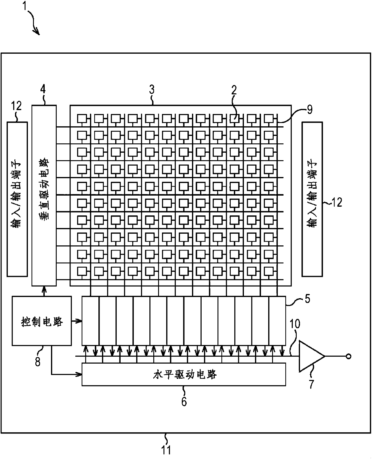
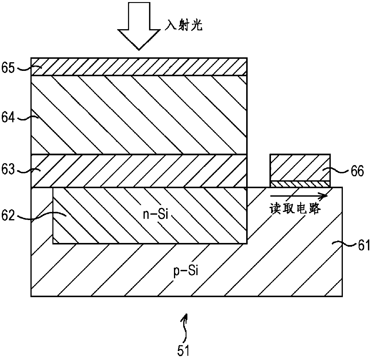
[0050] 1. First Embodiment (Example of Basic Solid-State Imaging Device of the Invention)
no. 2 example
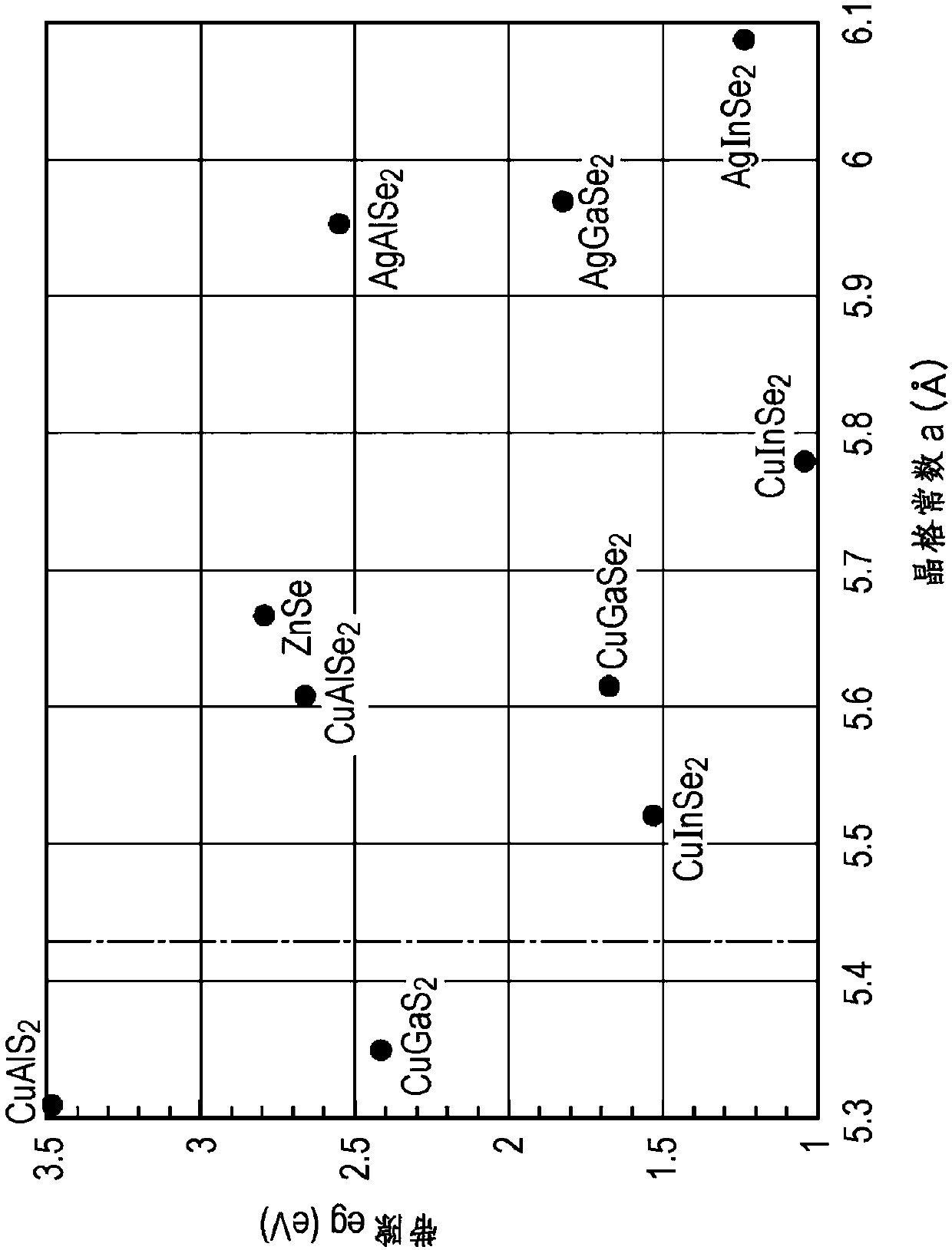
[0051] 2. Second Embodiment (Example of Solid-State Imaging Device Including Band Gaps of Various Colors)
no. 3 example
[0052] 3. Third Embodiment (Example of Solid-State Imaging Device Including Charge Blocking Layer)
Login to View More PUM
 Abstract
The invention relates to a solid state image sensor and an electronic apparatus. The solid state imaging device includes a photoelectric conversion device that includes a non-chalcopyrite-based compound semiconductor of at least one layer, which is lattice bonded or pseudo lattice bonded, and is formed on a silicon substrate, and a chalcopyrite-based compound semiconductor of at least one layer which is formed on the non-chalcopyrite-based compound semiconductor. According to the solid state image sensor and the electronic apparatus, even a chalcopyrite-based material with a high light absorbing coefficient is used as a photoelectric converting layer, high sensitivity can be realized and furthermore dark current is suppressed.
Description
[0001] This application is a divisional application of the patent application No. 201410758371.6 with the filing date of December 10, 2014 and the title of the invention being “Solid State Imaging Device and Electronic Device”. technical field [0002] The present invention relates to a solid-state imaging device and an electronic device, and particularly to a solid-state imaging device and an electronic device capable of suppressing dark current. Background technique [0003] As a solid-state imaging device (image sensor) using a semiconductor, a pn junction photodiode using a semiconductor is known. Such solid-state imaging devices are mounted on many electronic devices such as digital still cameras, video cameras, surveillance cameras, mobile terminals, optical sensors, and the like. [0004] Dark current can be said to be one of the properties of solid-state imaging devices. A solid-state imaging device performs photoelectric conversion from light to electricity on inci...
Claims
Login to View More Application Information
Patent Timeline
 Patent Type & Authority Applications(China)
IPC IPC(8): H01L27/146
CPCH01L27/14632H01L27/14645H01L31/09Y02E10/541H01L31/0322
Inventor 永广侯治
Owner SONY SEMICON SOLUTIONS CORP
Features
- R&D
- Intellectual Property
- Life Sciences
- Materials
- Tech Scout
- Unparalleled Data Quality
- Higher Quality Content
- 60% Fewer Hallucinations
Learn More Browse by: Latest US Patents, China's latest patents, Technical Efficacy Thesaurus, Application Domain, Technology Topic, Popular Technical Reports.
© 2025 PatSnap. All rights reserved.Legal|Privacy policy|Modern Slavery Act Transparency Statement|Sitemap|About US| Contact US: help@patsnap.com