Flexible display device and method for preparing the same
A flexible display device and flexible technology, applied in the direction of final product manufacturing, climate sustainability, sustainable manufacturing/processing, etc., can solve the problems of reducing the overall bending deformation of the screen, increasing the bending strength of the screen, and poor film formation. , to achieve the effect of improving reliability and use effect, good flexible bending effect, and improving bending resistance
- Summary
- Abstract
- Description
- Claims
- Application Information
AI Technical Summary
Problems solved by technology
Method used
Image
Examples
Embodiment 1
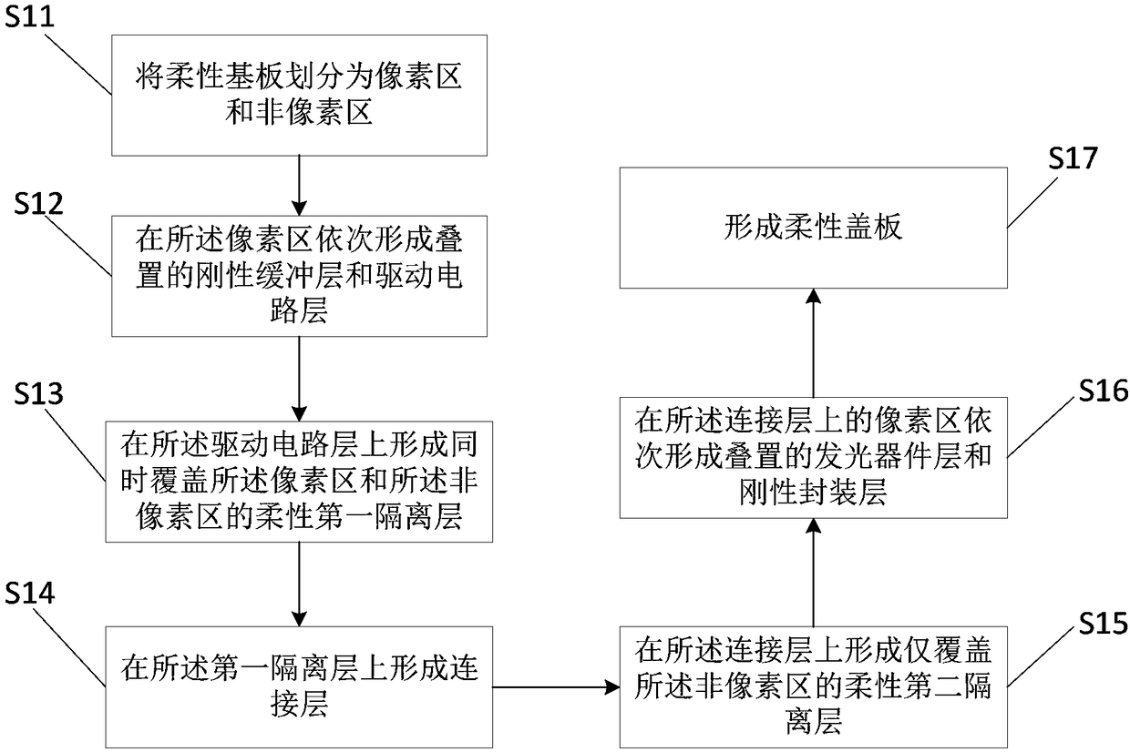
[0052] This embodiment provides a method for preparing a flexible display device, such as Figure 2-8 shown, including the following steps:
[0053] Step S11 , dividing the flexible substrate 1 into a pixel area 101 and a non-pixel area 102 .
[0054] Specifically, such as Figure 3-4 As shown, the flexible substrate 1 can be divided into a stacked two-layer structure, and a plurality of grooves 103 are formed on the upper flexible substrate 1 through a patterning process, and the region of the groove 103 is the pixel region 101, and the rest of the region is the non-pixel region. District 102. On the one hand, the recognition degree of the pixel area 101 and the non-pixel area 102 is improved, which is conducive to accurately distinguishing the pixel area 101 and the non-pixel area 102 during the preparation process, improving the preparation accuracy and reducing the difficulty of preparation; on the other hand, thinning The overall thickness of the display device is redu...
Embodiment 2
[0079] This embodiment provides a flexible display device prepared according to the preparation method in Embodiment 1, such as Figure 3-8 As shown, it includes a flexible substrate 1, a rigid buffer layer 2, a driving circuit layer 3, a flexible first isolation layer 4, a connection layer 5, a flexible second isolation layer 6, a light emitting device layer 8, a rigid packaging layer 9 and a flexible cover plate 10 .
[0080] The flexible substrate 1 is divided into a pixel area 101 and a non-pixel area 102 , and the rigid buffer layer 2 and the driving circuit layer 3 are sequentially stacked in the pixel area 101 of the flexible substrate 1 . The rigid buffer layer 2 can be an inorganic non-metallic material layer, generally, materials such as silicon nitride and silicon oxide can be used.
[0081] The flexible first isolation layer 4 is formed on the driving circuit layer 3 and covers the pixel area 101 and the non-pixel area 102 at the same time.
[0082] The connectio...
PUM
 Abstract
Description
Claims
Application Information


