Memory device, method for manufacturing memory device, and electronic device

A technology for memory devices and conductive layers, which is applied in the manufacture/processing of electromagnetic devices, electrical components, and field-controlled resistors, etc., and can solve problems such as low switching ratios and difficulty in meeting the needs of memory devices.

Pending Publication Date: 2018-07-27
QINGDAO RES INST OF BEIHANG UNIV
View PDF3 Cites 8 Cited by
  • Summary
  • Abstract
  • Description
  • Claims
  • Application Information

AI Technical Summary

Problems solved by technology

The lower switching ratio makes it difficult for MRAM in the prior art to...

Method used


Image

  • Memory device, method for manufacturing memory device, and electronic device
  • Memory device, method for manufacturing memory device, and electronic device
  • Memory device, method for manufacturing memory device, and electronic device

Examples


Embodiment Construction

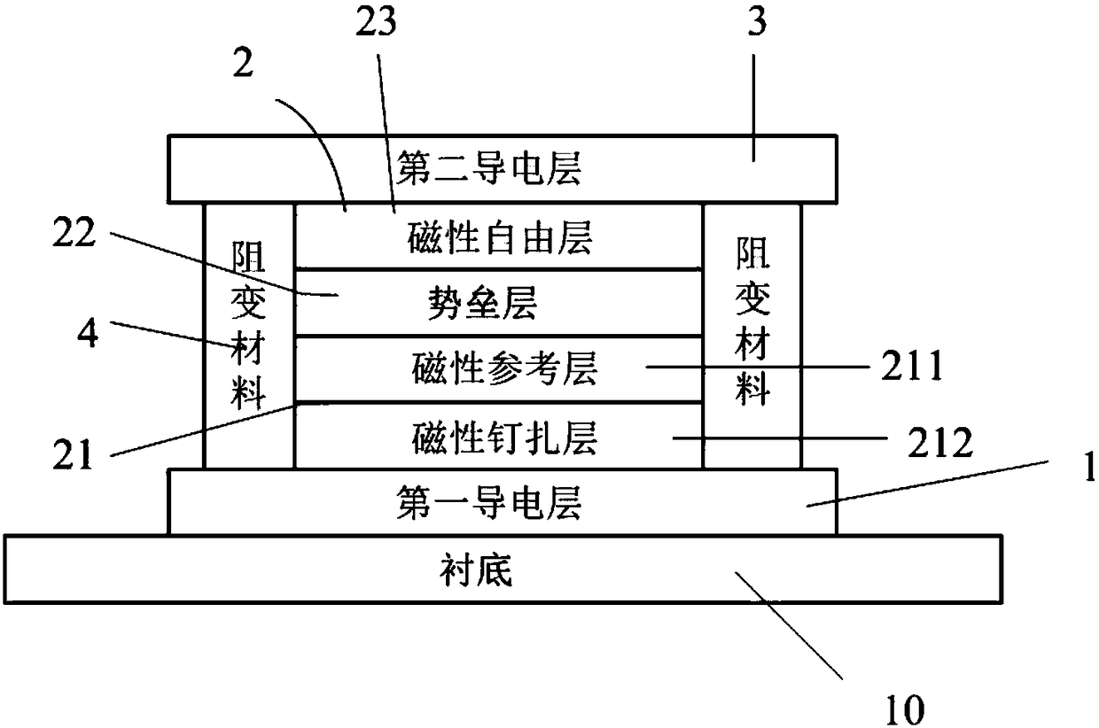
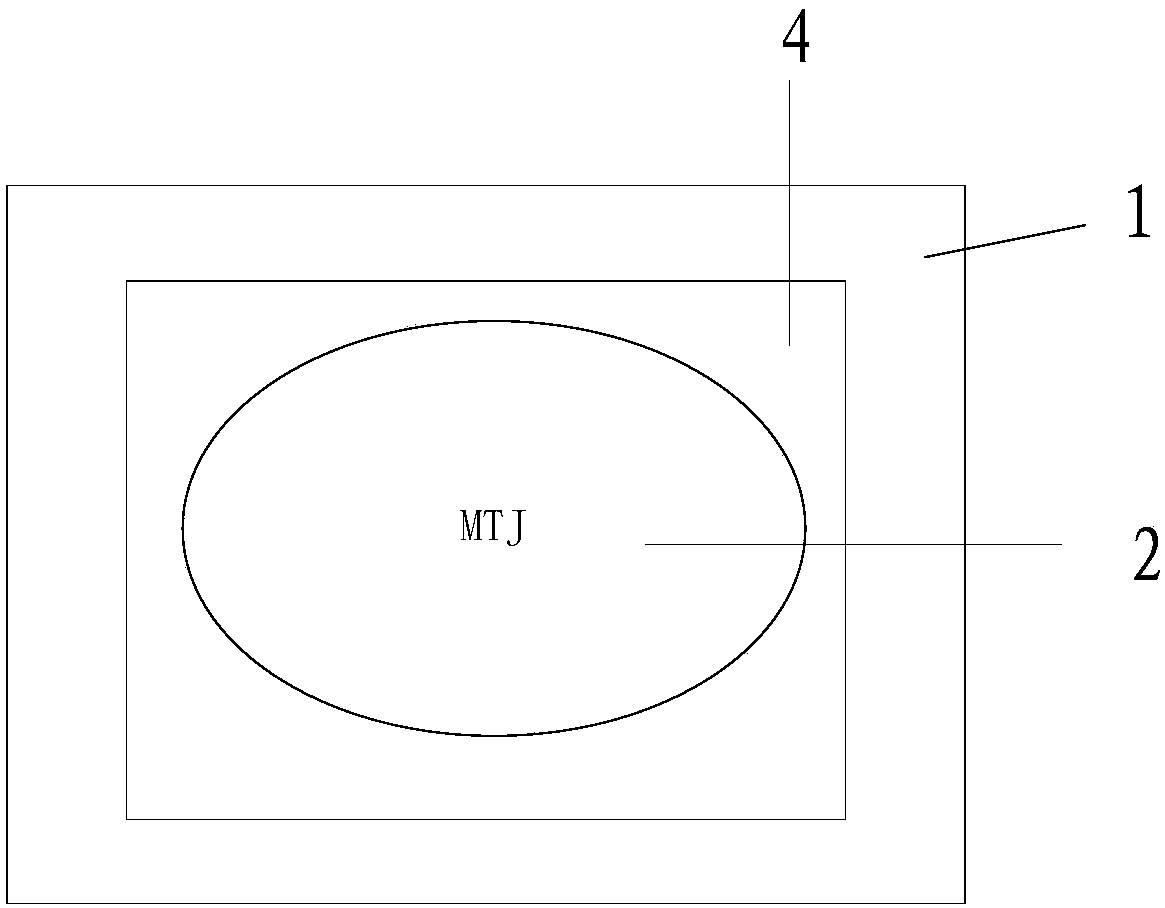
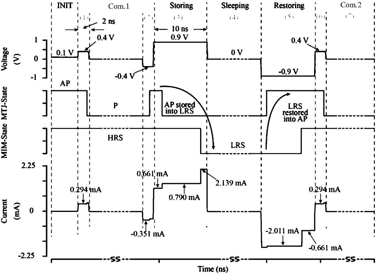
[0027] In order to make the purpose, technical solutions and advantages of the embodiments of the present invention clearer, the technical solutions in the embodiments of the present invention will be clearly and completely described below in conjunction with the drawings in the embodiments of the present invention. Obviously, the described embodiments It is a part of embodiments of the present invention, but not all embodiments. Based on the embodiments of the present invention, all other embodiments obtained by persons of ordinary skill in the art without making creative efforts belong to the protection scope of the present invention.

[0028] Terms used in the embodiments of the present invention are only for the purpose of describing specific embodiments, and are not intended to limit the present invention. The singular forms "a", "said" and "the" used in the embodiments of the present invention and the appended claims are also intended to include plural forms, unless the ...


PUM


Abstract

The embodiment of the invention provides a memory device, a manufacturing method of the memory device and an electronic device. The memory device comprises a resistive material, a first conductive layer sequentially stacked, a magnetic tunnel junction and a second conductive layer, wherein the first conductive layer, the magnetic tunnel junction and the second conductive layer are sequentially stacked; the resistive material is positioned between the first conductive layer and the second conductive layer; the resistive material is adhered to the edge of the magnetic tunnel junction to wrap themagnetic tunnel junction; the magnetic tunnel junction comprises a magnetic fixing layer, a barrier layer and a magnetic free layer which are sequentially stacked; a conductive channel is formed in the region near the magnetic tunnel junction in the resistive material and two ends of the conductive channel are respectively connected to the magnetic fixing layer and the magnetic free layer. The memory device provided by the embodiment of the invention can equivalently be the parallel connection of the magnetic memory unit and the impedance memory unit in the electrical structure, and has the advantages of high read-write speed, unlimited read-write operation, high switching ratio and the like.

Description

technical field [0001] The invention relates to the technical field of semiconductors, in particular to a storage device, a method for preparing the storage device and electronic equipment. Background technique [0002] At present, Magnetic Random Memory (MRAM) is a new type of non-volatile memory, which does not require continuous power supply during the data storage process, and can reduce the influence of leakage current during the data retention process of the device. [0003] Although MRAM has magnetoresistive characteristics, and has the characteristics of fast read and write speed, unlimited read and write operations, and radiation protection, the ON / OFF ratio of MRAM is relatively low. The low switching ratio makes it difficult for the MRAM in the prior art to meet the demand for higher performance memory devices in practical applications. Contents of the invention [0004] Embodiments of the present invention provide a storage device, a method for preparing a sto...

Claims


Application Information

Patent Timeline
IPC IPC(8): H01L43/08H01L43/12H01L45/00
CPCH10N50/01H10N70/24H10N50/10H10N70/011
Inventor 张雨赵巍胜林晓阳康旺张有光
Owner QINGDAO RES INST OF BEIHANG UNIV
Why Eureka
Try Eureka