Oxide semiconductor thin-film transistor and preparation method thereof

A technology of oxide semiconductors and thin film transistors, which is applied in the field of new oxide thin film transistors and its preparation, can solve the problems of limited reserves, achieve small sub-threshold swing, high practical value, and improve the driving ability of TFT

Inactive Publication Date: 2012-08-15
PEKING UNIV
View PDF4 Cites 7 Cited by
  • Summary
  • Abstract
  • Description
  • Claims
  • Application Information

AI Technical Summary

Problems solved by technology

However, due to the extremely limited reserves of indium (In) in the world, IGZO is only a temporary choice, and other oxide semiconductor materials must be developed to replace IGZO

Method used


Image

  • Oxide semiconductor thin-film transistor and preparation method thereof
  • Oxide semiconductor thin-film transistor and preparation method thereof
  • Oxide semiconductor thin-film transistor and preparation method thereof

Examples


Embodiment Construction

[0024] Below in conjunction with the accompanying drawings of the description, the present invention will be further described by examples.

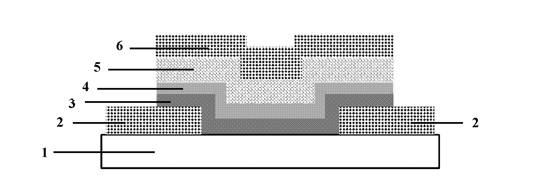
[0025] The zinc aluminum oxide thin film transistor of the present invention is formed on the glass substrate, as figure 1 and figure 2 shown. The thin film transistor includes a source electrode and a drain electrode, an active area, a gate dielectric layer and a gate electrode. The source and drain electrodes are located on the substrate, the active area is located on the substrate and the source and drain electrodes, the gate dielectric layer is located on the active area, and the gate electrode is located on the gate dielectric layer.

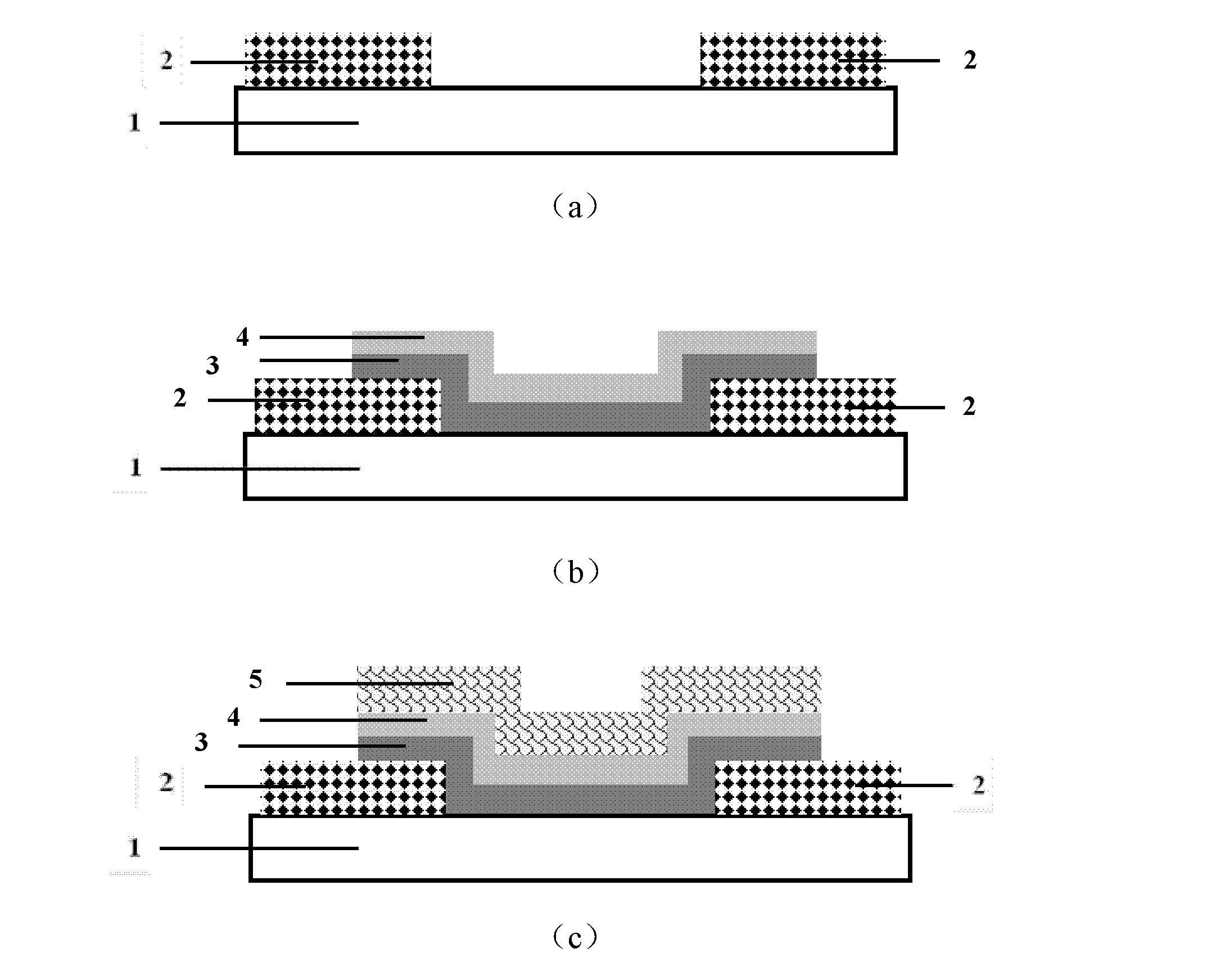
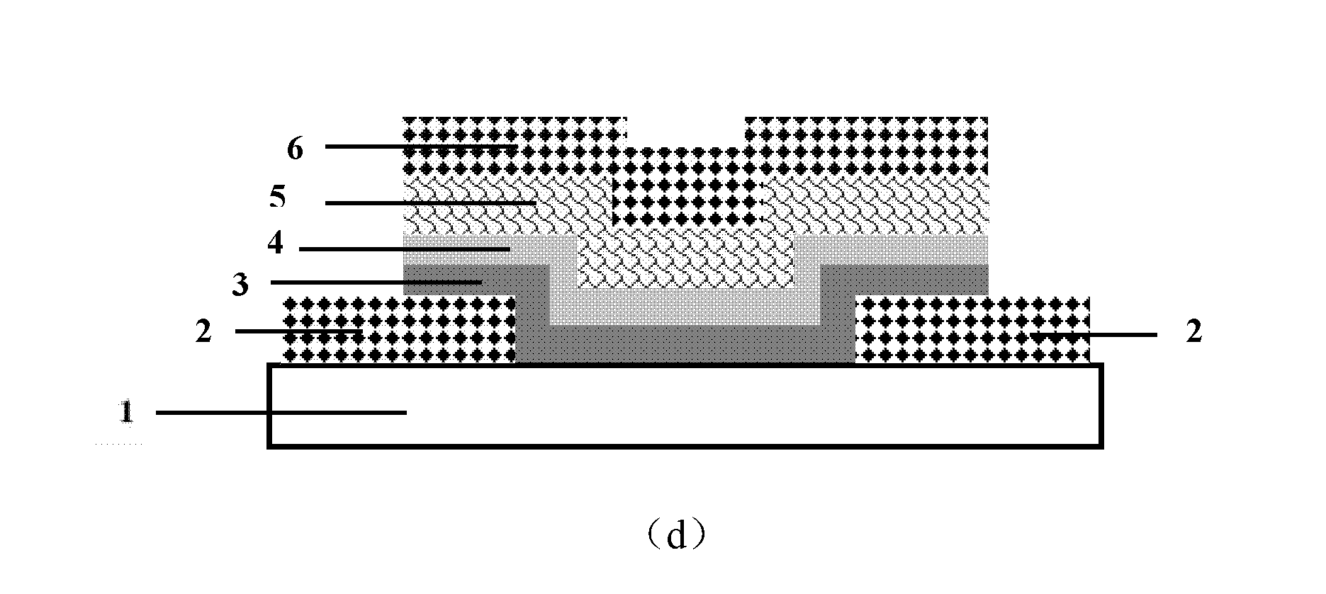
[0026] An embodiment of the preparation method of the zinc-aluminum oxide thin film transistor of the present invention consists of figure 2 (a) to figure 2 (d), including the following steps:

[0027] (1) Magnetron sputtering grows a layer of transparent conductive metal oxide ITO film with a...


PUM


Abstract

The invention discloses an oxide semiconductor thin-film transistor and a preparation method for the oxide semiconductor thin-film transistor, belonging to the technical fields of semiconductor integrated circuits and manufacturing of the semiconductor integrated circuits. Two layers of AlZnO thin-film materials are formed as active areas by adoption of a radio frequency magnetron sputtering method, and the two layers of the AlZnO thin-film materials contain different oxygen ion contents. The oxide semiconductor thin-film transistor disclosed by the invention has the advantages of high migration rate. The preparation method disclosed by the invention and the existing CMOS (complementary metal-oxide-semiconductor transistor) technology are compatible, so that the preparation method has higher practical value, and can be applied in future TFT (thin-film transistor) integrated circuits.

Description

technical field [0001] The invention belongs to the field of integrated circuit manufacturing and flat panel display, and specifically relates to a novel oxide thin film transistor and a preparation method thereof. Background technique [0002] With the development of integrated circuit manufacturing and flat panel display technology, it is extremely important to improve the performance of thin film transistors (TFT) and reduce its production cost to promote the development of flat panel display. Currently, amorphous silicon (a-Si) and low-temperature polysilicon (LTPS) technologies are mainly used in manufacturing various display TFT devices and driving circuits in the industry. The biggest difference between LTPS-TFT and a-Si-TFT is the conductive characteristics and preparation process. LTPS-TFT has high carrier mobility, can provide sufficient current, and can prepare n-type and p-type TFTs. However, due to the complex preparation process, laser or metal-induced recrys...

Claims


Application Information

Patent Timeline
Patent Type & Authority Applications(China)
IPC IPC(8): H01L29/78H01L21/336
Inventor 韩德栋王漪蔡剑王亮亮任奕成张盛东孙雷刘晓彦康晋锋
Owner PEKING UNIV
Why Eureka
Try Eureka