

Electret-based synapse transistor and preparation method thereof
An electret and transistor technology, which is applied in the field of electret-based synaptic transistors and their preparation, can solve problems such as the lack of synaptic transistors, and achieve the effects of high switching ratio and improved accuracy
- Summary
- Abstract
- Description
- Claims
- Application Information
AI Technical Summary
Problems solved by technology
Method used
Image

Examples
preparation example Construction
[0029] Preferably, this embodiment also provides a method for preparing an electret-based synaptic transistor, comprising the following steps:
[0030] Step S1: cleaning the substrate, ie cleaning the substrate with the insulating layer;
[0031] Step S2: Dissolving the organic electret material in an organic solvent in a certain proportion, fully heating and stirring, after fully dissolving, spin-coat a uniform film on the substrate, and perform annealing treatment under air conditions to obtain an electret polar body dielectric layer;
[0032] Step S3: The organic macromolecular copolymer material is dissolved in an organic solvent in a certain proportion, fully heated and stirred, and continued on the electret layer by spin coating or scraping coating, and then annealed under air conditions to obtain organic semiconductor layer;
[0033] Step S4: Evaporate a layer of top electrode on the organic semiconductor layer through a mask plate by vacuum evaporation deposition.
...
Embodiment 1
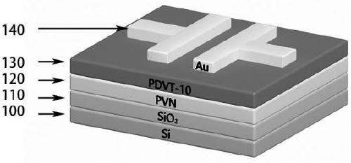
[0039] Step 1: Cut the SiO with 100 nm 2 The silicon wafers were soaked in acetone and isopropanol for 2 min, washed with deionized water, and then dried with nitrogen to obtain clean silicon wafers. figure 1 Parts (100) and (110).
[0040] Step 2: Prepare polymer electret poly(2-vinylnaphthalene) (PVN) at 3 mg·mL -1 The concentration was dissolved in toluene solvent with a purity of 99.99%, placed on a heating platform, and heated at 60 °C for 2 h until it was completely dissolved.
[0041] Step 3: Prepare the polymer semiconductor material PDVT-10 at 5 mg·mL -1 The concentration was dissolved in chlorobenzene solvent, then heated, heated at 60 °C and stirred at 500 rpm for 12 h.
[0042] Step 4: Take about 0.1 mL of PVN solution with a rubber dropper, slowly drop it on the cleaned Si substrate, cover the substrate completely and start spin coating, the spin coating speed is 3000 rpm, and the rotation acceleration is 500 rpm / s, the spin coating time is 60 s. After stand...
Embodiment 2
[0046] Step 1: Cut the SiO with 100 nm 2 The silicon wafers were soaked in acetone and isopropanol for 2 min, then washed with deionized water, repeated three times, ultrasonically cleaned three times, and then dried with nitrogen to obtain clean silicon wafers.
[0047] Step 2: Configure polymer electret PVN to 5mg·mL -1 The concentration was dissolved in toluene solvent with a purity of 99.99%, placed on a heating platform, and heated at 60 °C for 2 h until it was completely dissolved.
[0048] Step 3: Prepare polymer semiconductor material ID-TBT at 10 mg·mL -1 The concentration was dissolved in chloroform solvent, then heated, heated at 60°C and stirred at 500 rpm for 12 h.
[0049] Step 4: Take the fully dissolved PVN solution with a 1ml syringe, slowly drop it on the cleaned Si substrate, and start spin coating after covering the substrate completely. The spin coating speed is 3000 rpm, and the rotation acceleration is 500 rpm / s. The spin coating time was 60 s. Let i...
PUM
| Property | Measurement | Unit |
|---|---|---|
| thickness | aaaaa | aaaaa |
| thickness | aaaaa | aaaaa |
| thickness | aaaaa | aaaaa |
Abstract
Description
Claims
Application Information