Three-dimensional (3D) oxide semiconductor thin film transistor and preparation method thereof

A technology of oxide semiconductor and thin film transistor, which is applied in semiconductor/solid-state device manufacturing, transistors, semiconductor devices, etc., can solve the problems of limited storage, high toxicity, high cost, etc. The effect of current and cost reduction

Active Publication Date: 2012-10-03
BOE TECH GRP CO LTD
View PDF5 Cites 7 Cited by
  • Summary
  • Abstract
  • Description
  • Claims
  • Application Information

AI Technical Summary

Problems solved by technology

However, since indium is a rare metal with very limited storage capacity, it is expensive and highly toxic, so it is necessary to find a material that can replace IGZO

Method used


Image

  • Three-dimensional (3D) oxide semiconductor thin film transistor and preparation method thereof
  • Three-dimensional (3D) oxide semiconductor thin film transistor and preparation method thereof
  • Three-dimensional (3D) oxide semiconductor thin film transistor and preparation method thereof

Examples


Embodiment Construction

[0028] Below in conjunction with the accompanying drawings of the description, the present invention will be further described by examples.

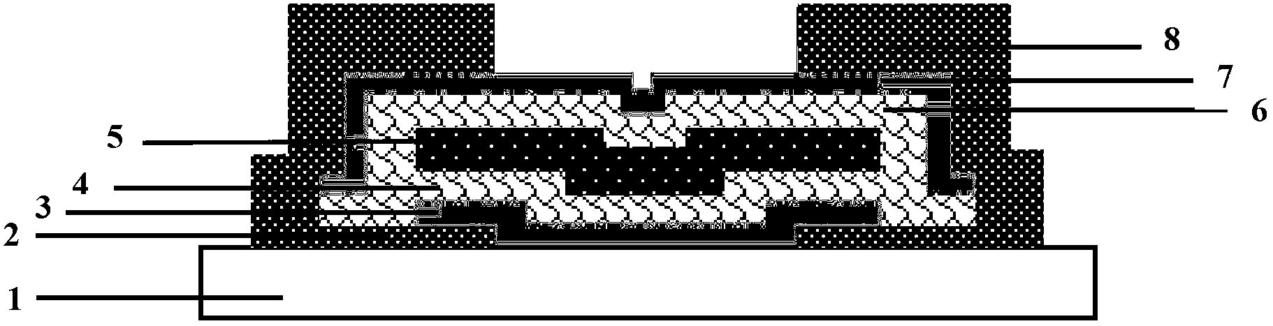
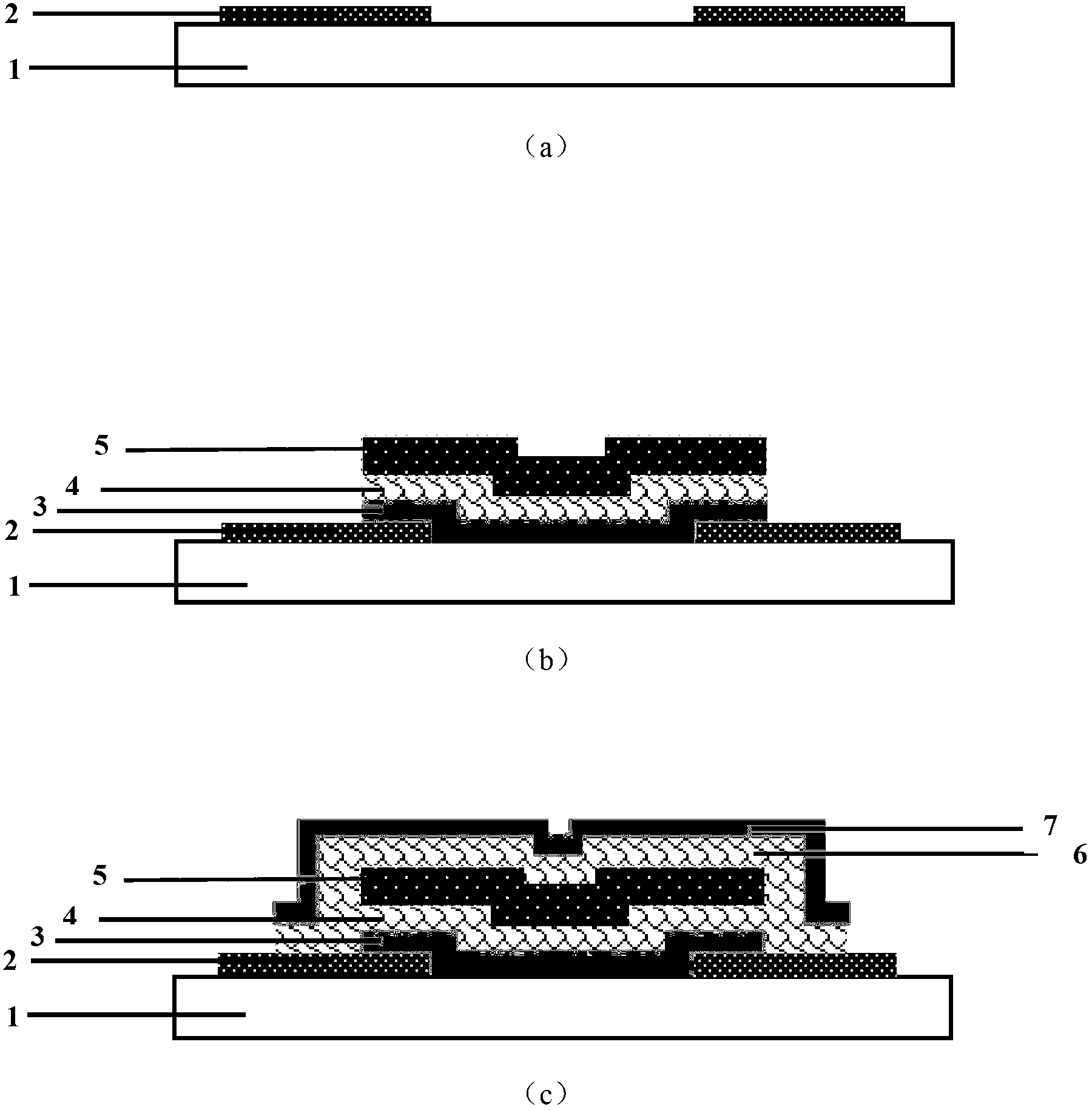
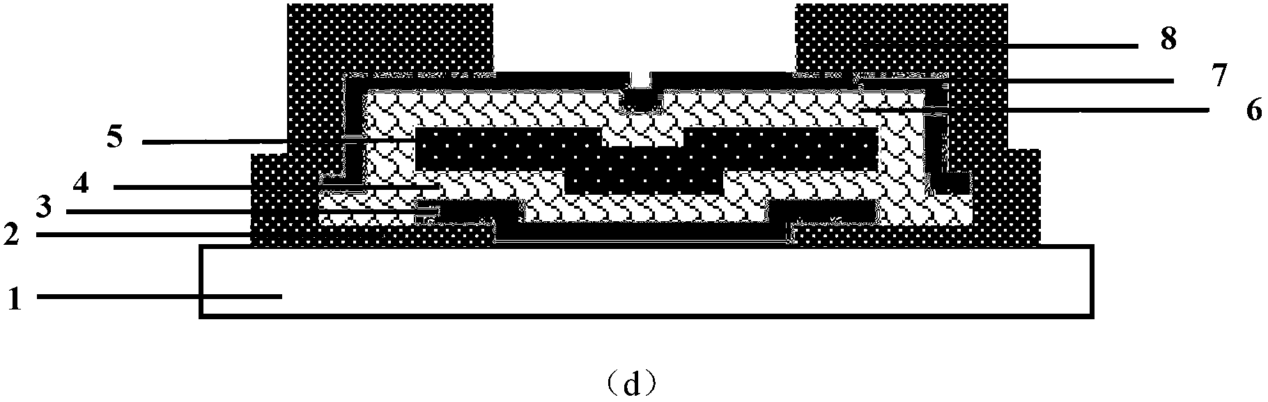
[0029] The zinc aluminum oxide thin film transistor of the present invention is formed on the substrate of glass, as figure 1 and figure 2 shown. The 3D oxide semiconductor thin film transistor of the present invention includes: a lower source electrode and a lower drain electrode 2, a lower active region 3, a lower gate dielectric 4, a gate electrode 5, an upper gate dielectric 6, an upper active region 7, and an upper source electrode and an upper layer drain electrode 8; wherein, a lower layer source electrode and a lower layer drain electrode 2 are formed at both ends on the substrate 1, and a lower layer active region 3 is formed on the substrate 1 and part of the lower layer source electrode and the lower layer drain electrode 2, A lower gate dielectric 4 is formed on the lower active region 3, a gate electrode 5 is formed on th...


PUM


Abstract

The invention discloses a three-dimensional (3D) oxide semiconductor thin film transistor (TFT) and a preparation method thereof. According to the TFT, the continuous growth of a lower-layer active area, a lower-layer gate dielectric and a gate electrode and the continuous growth of an upper-layer gate dielectric and an upper-layer active area are adopted, so that the interface deficiency state of an active layer and the gate dielectric can be greatly reduced to greatly improve the driving capability of the (TFT). Moreover, the same gate electrode can simultaneously control the upper-layer and lower-layer active areas, so that the driving capability of the TFT is further improved. The TFT prepared by the method has the good characteristics of high switch ratio, high on-state current, abrupt sub-threshold slope and the like. Therefore, the TFT and the preparation method thereof have high practical value, and are expected to be widely used for microelectronic and flat panel display industries. Furthermore, if the upper-layer and lower-layer active areas are controlled by different threshold voltages, a multi-threshold technology can be integrated into the same TFT, and the integration of the multi-threshold technology into the TFT is expected to widely used for pixel driving unit circuits.

Description

technical field [0001] The invention belongs to the field of flat panel display, and in particular relates to a 3D oxide semiconductor thin film transistor and a preparation method thereof. Background technique [0002] At present, in the field of flat panel display of organic light emitting diode OLED pixel drive unit, the application of oxide semiconductor thin film transistor OSTFT has become more and more mature. Compared with amorphous silicon a-Si and low-temperature polysilicon LTPS technology, it has obvious advantages: 1. Zinc oxide and its doped semiconductor material thin film transistor has high mobility to adapt to OLED display mode, fast ultra-large screen liquid crystal display mode and 3D display 2. Zinc oxide and its doped semiconductor material thin film transistors are amorphous materials with good and consistent electrical characteristics; 3. Zinc oxide and its doped semiconductor material thin film transistors are compatible with the current flat panel d...

Claims


Application Information

Patent Timeline
Patent Type & Authority Applications(China)
IPC IPC(8): H01L29/423H01L29/10H01L29/786H01L21/28H01L21/336
Inventor 王漪蔡剑韩德栋王亮亮任奕成张盛东孙雷刘晓彦康晋锋
Owner BOE TECH GRP CO LTD
Why Eureka
Try Eureka