

Indium tin zinc oxide homogeneous thin film transistor and preparation method thereof
A thin-film transistor and oxide technology, applied in transistors, semiconductor/solid-state device manufacturing, semiconductor devices, etc., can solve the problems that cannot be applied to popular display products, cannot meet the requirements of driving OLED, and the preparation process is complicated, and achieves easy injection and visible light. The effect of transparency and simplified preparation process
- Summary
- Abstract
- Description
- Claims
- Application Information
AI Technical Summary
Problems solved by technology
Method used
Image

Examples
preparation example Construction
[0037] The preparation method of the above-mentioned indium tin zinc oxide homogeneous thin film transistor comprises the following steps:
[0038] 1) Ultrasonic cleaning of glass or flexible substrates, the cleaning liquid is semiconductor cleaning agent, absolute alcohol, acetone, and then dried with high-purity nitrogen;
[0039] 2) Prepare the gate on the substrate by magnetron sputtering, electron beam evaporation and other methods. The gate material can be Al, Mo, Cr, Cu, Ni, Ta, Ag, Au, Ti, Pt and other metal materials. Indium tin oxide (ITO), aluminum-doped zinc oxide (AZO), IGZO, ITZO and other metal oxide materials can also be used. The thickness of the gate is 100~400 nm, and it can be formed by masking or photolithography;
[0040] 3), and then use magnetron sputtering, atomic layer deposition (ALD), plasma enhanced chemical vapor deposition (PECVD) and other methods to prepare the insulating layer, the insulating layer material can be aluminum oxide, hafnium oxide, ...
Embodiment 1
[0051] The atomic number ratio of indium, tin, and zinc is a:b:c=87.44:9.15:3.41 In 2 o 3 , SnO 2 Mix with ZnO powder evenly, and then make ITZO ceramic target through molding, sintering, machining and grinding; the sintering temperature is 1000-1200℃.
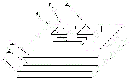
[0052] Using the ITZO ceramic target in this example to prepare a structure such as figure 1 The homogeneous ITZO-TFT shown, where the substrate is a thermally oxidized silicon wafer, where Si is used as the gate and substrate, and SiO 2 As an insulating layer, the thickness is 200 nm; the channel layer is prepared by magnetron sputtering method, the target used for sputtering is the ITZO ceramic target prepared in this example, and the background vacuum of sputtering is 1×10 -4 Pa, the sputtering gas is Ar / O 2 Mixed gas, the flow rate of argon gas is 50 sccm, the flow rate of oxygen gas is 5 sccm, the gas pressure is 0.6 Pa, the sputtering power is 60 W, the thickness of the prepared channel layer is 30 nm, and it is for...
Embodiment 2
[0054] The atomic number ratio of indium, tin, and zinc is a:b:c=55.17:21.16:23.67 In 2 o 3 , SnO 2 Mix with ZnO powder evenly and then make ITZO ceramic target through molding, sintering, machining and grinding;
[0055] Using the ITZO target in this example to prepare a structure such as figure 1 Homogeneous ITZO-TFT shown. The substrate is a thermally oxidized silicon wafer, where Si is used as the gate and substrate, and SiO 2 As an insulating layer, the thickness is 200 nm; the channel layer is prepared by magnetron sputtering method, the target used for sputtering is the ITZO target prepared in this example, and the background vacuum of sputtering is 1×10 -4 Pa, the sputtering gas is Ar / O 2 Mixed gas, the flow rate of argon gas is 50 sccm, the flow rate of oxygen gas is 5 sccm, the gas pressure is 0.6 Pa, the sputtering power is 60 W, the thickness of the prepared channel layer is 30 nm, and it is formed by mask method; the source and drain electrodes are formed by...
PUM
| Property | Measurement | Unit |
|---|---|---|
| Thickness | aaaaa | aaaaa |
| Thickness | aaaaa | aaaaa |
| Thickness | aaaaa | aaaaa |
Abstract
Description
Claims
Application Information