Semiconductor laser chip package precision detection method and device

A technology for chip packaging and precision testing, which is applied in the direction of measuring devices, optical devices, instruments, etc., can solve the problems that do not involve the detection function of semiconductor laser chip packaging precision, does not involve the detection function of chip packaging precision, etc., and achieves fast detection speed , Good detection effect, accurate detection effect

Inactive Publication Date: 2018-08-10
Shandong Huaguang Optoelectronics Co. Ltd.
View PDF8 Cites 4 Cited by
  • Summary
  • Abstract
  • Description
  • Claims
  • Application Information

AI Technical Summary

Problems solved by technology

[0006] Chinese patent document CN104075873A discloses a semiconductor laser spot detection device and method, which uses the collimation of the laser and the lens system to detect the spot of the semiconductor laser by judging the spot of the high-power semiconductor laser packaged in C-mount, but the method mainly It is aimed at testing the spot quality of high-power packaged semiconductor lasers, especially C-mount packaged semiconductor lasers, which are quite different from TO packaged semiconductor lasers in terms of structure and method, and does not involve the detection of chip package accuracy of TO packaged semiconductor lasers. effect
[0007] Chinese patent document CN2004100512275 discloses a detection method of a semiconductor laser die through a central control computer, a set of laser die drive circuits, a set of data acquisition circuits, and a laser die containing a laser die test fixture It consists of a probe station for detection, two detectors for the front light output and the rear light output, and a set of temperature control circuits. The computer is connected to the laser die drive circuit, data acquisition circuit, and temperature control circuit through a common interface. ; One end of the probe of the probe station is connected to the laser die drive circuit through wires; the two detectors are respectively connected to the data acquisition circuit through wires, which realizes the display of the laser chip test data on the computer, and makes the electrical parameters of the laser chip Comprehensive evaluation; however, it does not involve the detection of semiconductor laser chip packaging accuracy

Method used


Image

  • Semiconductor laser chip package precision detection method and device
  • Semiconductor laser chip package precision detection method and device
  • Semiconductor laser chip package precision detection method and device

Examples


Embodiment Construction

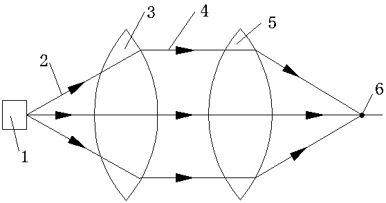
[0024] The present invention utilizes the convex lens to have light-gathering effect on the light, and realizes that the elliptical light shape emitted by the laser is focused after passing through the convex lens; according to the shape difference of the focused light spot of different light-emitting points after being focused by two convex lenses, it is detected near the focal point The shape of the light spot can realize the detection of the accuracy of the position of the laser light-emitting point—that is, the detection of the packaging accuracy of the laser chip.

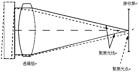
[0025] like figure 1 As shown, the emitted light 2 of the semiconductor laser 1 will become parallel light 4 after passing through the first convex lens 3 , and the light after the parallel light 4 is focused by the second convex lens 5 finally becomes a focused light spot 6 on the receiving screen.

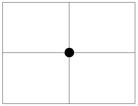
[0026] Ideally, the light emitting point of the chip is located on the optical axis of the convex lens, and th...


PUM


Abstract

The invention provides a semiconductor laser chip package precision detection method and device. The method is characterized in that light output by a semiconductor laser chip is incident to a first convex lens to form parallel rays; the parallel rays are incident to a second convex lens in a manner of being parallel to the principal optical axis of the second convex lens, the principal optical axes of the first convex lens and the second convex lens being overlapped; the parallel rays are focused to one point on the principal optical axis after passing through the second convex lens, and by detecting the shape of the focusing light point, package precision of the semiconductor laser chip is judged. The device comprises a support, a driving power supply, a sleeve, a convex lens group and alight spot receiving screen. The driving power supply is arranged on the support; the sleeve is horizontally mounted on the support; the convex lens group is embedded in the front portion of a sleeveinner hole; the back portion of the sleeve inner hole is a semiconductor laser plug hole; the principal optical axes of the convex lenses and the axis of the semiconductor laser plug hole are overlapped; and the light spot receiving screen is arranged on the support. The semiconductor laser chip package precision detection method and device are good in detection effect, accurate in detection andfast in detection speed.

Description

technical field [0001] The invention relates to a method and a device for detecting the packaging accuracy of semiconductor laser chips, in particular to the detection of chip placement accuracy of TO packaged visible light lasers, and belongs to the technical field of semiconductor laser packaging. Background technique [0002] The requirement of semiconductor laser chip packaging accuracy is an essential process step in semiconductor device packaging and manufacturing, and it is also a very important process. The quality of the process not only affects the photoelectric conversion efficiency of semiconductor devices, but also directly affects the device. Reliability and life, but also cause certain adverse effects on the use of semiconductor lasers. [0003] Semiconductor lasers are the most important class of lasers in practice. It has the characteristics of small size, long life, low power consumption, low price, etc., and can be pumped by a simple way of injecting curr...

Claims


Application Information

Patent Timeline
Patent Type & Authority Applications(China)
IPC IPC(8): G01B11/00
Inventor 梁盼张骋汤庆敏徐现刚
Owner Shandong Huaguang Optoelectronics Co. Ltd.
Why Eureka
Try Eureka