Thin type light guide structure and method for assembling thin type light supply module
A light guide structure and assembly method technology, applied in the direction of light guide, optics, optical components, etc., to achieve the effect of increasing mass production speed and increasing process speed
- Summary
- Abstract
- Description
- Claims
- Application Information
AI Technical Summary
Problems solved by technology
Method used
Image
Examples
Embodiment 1
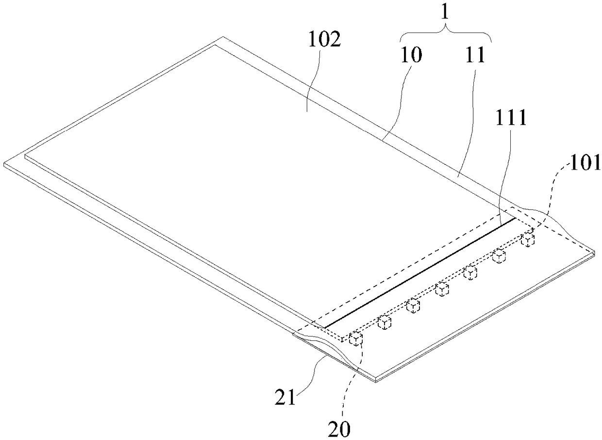
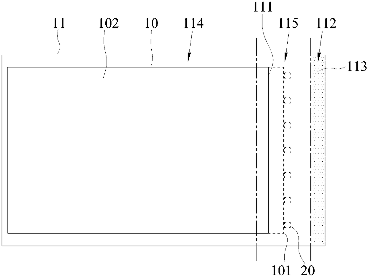
[0053] Such as figure 1 , figure 2 and image 3 As shown, it is an assembly schematic diagram, an assembly side view schematic diagram and an assembly top view schematic diagram of Embodiment 1 of the present invention. The present invention here discloses a thin light guide structure 1 for use with a plurality of LEDs 20 , and the LEDs 20 are arranged on a substrate 21 . The aforementioned thin light guide structure 1 includes a light guide plate 10 and a reflective sheet 11 .
[0054]The light guide plate 10 has a light incident surface 101, and as mentioned above, the light guide plate 10 can be a light guide plate with an extremely thin thickness. In this embodiment, the thickness of the light guide plate 10 is less than 0.3mm. Preferably, the thickness can be further selected. The light guide plate is about 0.2mm. The reflective sheet 11 has a mounting gap 111 and a bonding area 112, and the opposite sides of the reflective sheet 11 are reflective layers. Preferably...
Embodiment 2
[0060] Such as Figure 5 and Figure 6A ~ Figure 6C As shown, it is a flow chart of steps and a schematic diagram of each assembly step of Embodiment 2 of the present invention. In this embodiment, an assembly method of the thin light supply module 2 is disclosed, which includes the following steps. Firstly, a thin light guide structure 1 as mentioned above is provided. The thin light guide structure 1 includes a light guide plate 10 and a reflective sheet 11, wherein the light guide plate 10 has a light incident surface 101, and the reflective sheet 11 has an installation slit 111 and a bonding area 112, and the opposite sides of the reflective sheet 11 are reflective layers (step S01), such as Figure 6A shown. Next, the side of the light guide plate 10 with the light incident surface 101 is inserted through the installation gap 111, so that the light guide plate 10 and the reflection sheet 11 are stacked in a staggered manner (step S02), as shown in FIG. Figure 6B show...
PUM
 Abstract
Description
Claims
Application Information


