SOI NMOS total-dose radiation multi-offset point current model establishing method

A technology of total dose radiation and current model, which is applied in electrical digital data processing, special data processing applications, instruments, etc., can solve the problems of long cycle and high cost of total dose radiation effect research

Active Publication Date: 2018-08-10
SHANGHAI INST OF MICROSYSTEM & INFORMATION TECH CHINESE ACAD OF SCI
View PDF5 Cites 8 Cited by
  • Summary
  • Abstract
  • Description
  • Claims
  • Application Information

AI Technical Summary

Problems solved by technology

[0006] In view of the above-mentioned shortcomings of the prior art, the object of the present invention is to provide a SOI NMOS total dose radiation multi-bias point current model modeling method, which is used to solve the problem of high cost and long period of total dose radiation effect research in the prior art. And other issues

Method used


Image

  • SOI NMOS total-dose radiation multi-offset point current model establishing method
  • SOI NMOS total-dose radiation multi-offset point current model establishing method
  • SOI NMOS total-dose radiation multi-offset point current model establishing method

Examples


Embodiment 1

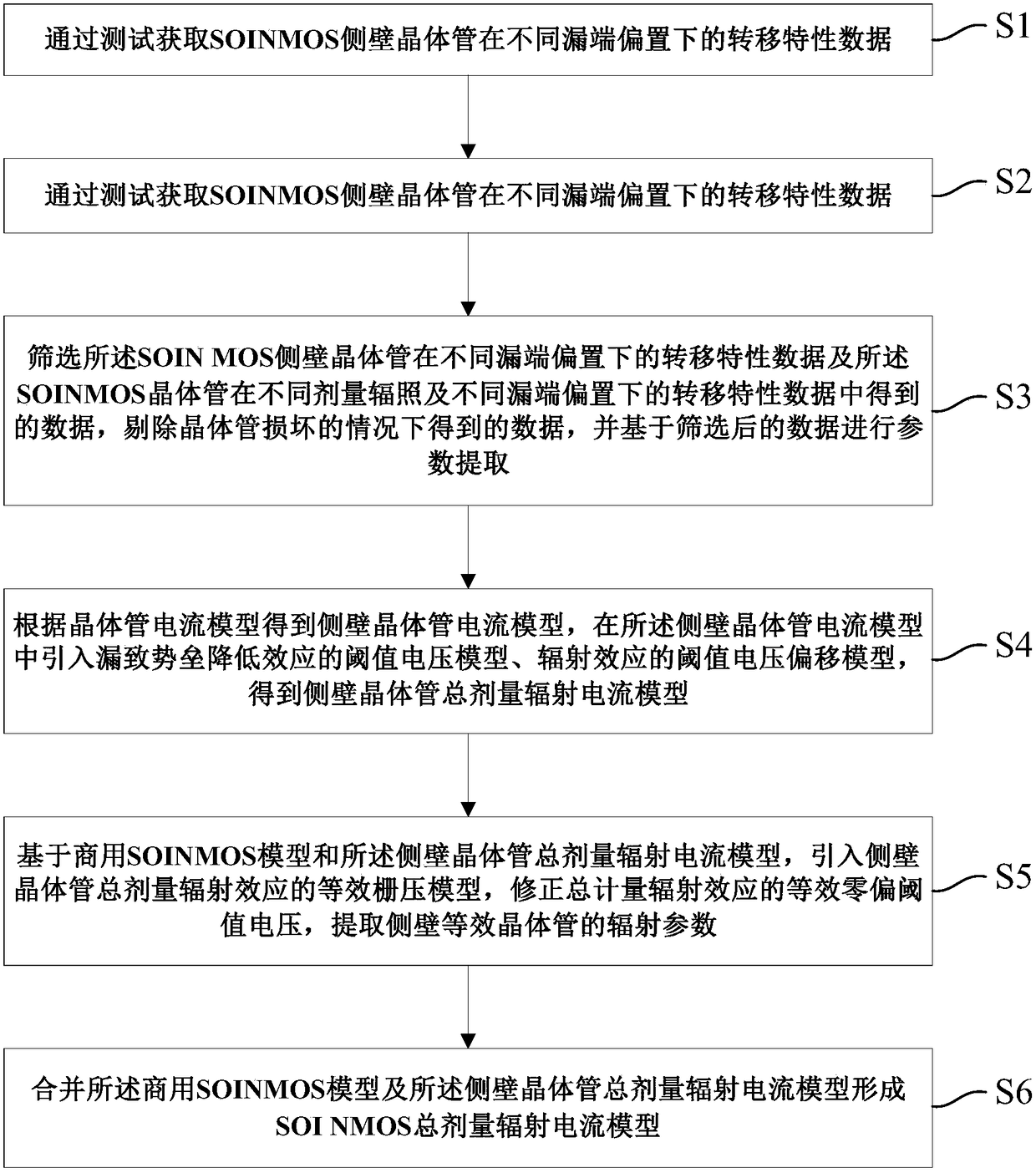
[0062] Such as image 3 As shown, the present invention provides a SOI NMOS total dose radiation multi-bias point current model modeling method, and the SOI NMOS total dose radiation multi-bias point current model modeling method includes:

[0063] Step S1: Obtain transfer characteristic data of the SOI NMOS sidewall transistor under different drain biases through testing.

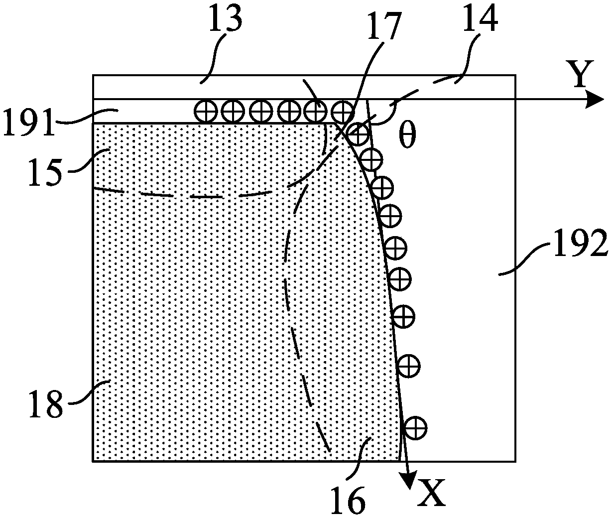
[0064] Specifically, an SOI NMOS sidewall transistor is provided, and different drain terminal bias voltages are respectively provided to the SOI NMOS sidewall transistors, and the sidewall gate terminal of the SOI NMOS sidewall transistor is changed under each drain terminal bias voltage The test voltage applied on the gate is used to obtain the corresponding drain current, and then the corresponding relationship between the gate voltage and the drain current under different drain biases is obtained.

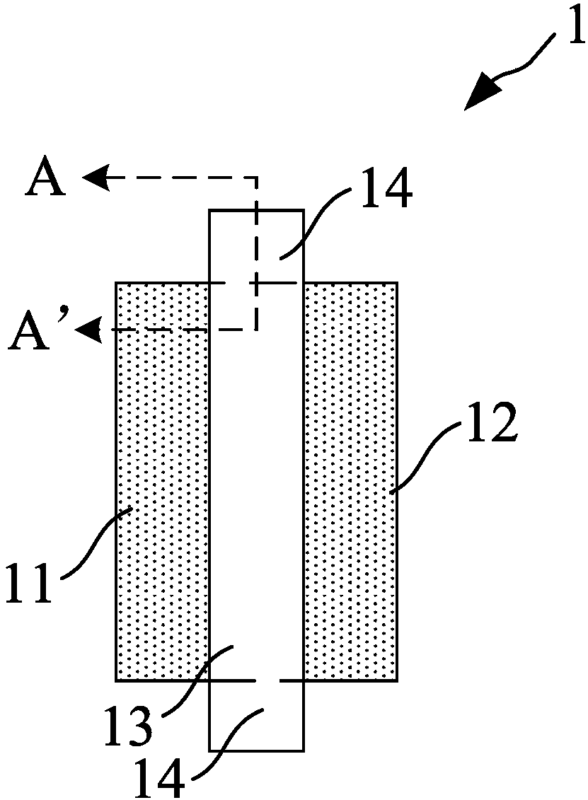
[0065] More specifically, as Figure 4 As shown, in this embodiment, the width-to-length ratio W / L of ...

Embodiment 2

[0093] This embodiment provides a SOI NMOS total dose radiation multi-bias point current model modeling method, which differs from Embodiment 1 in that step S1, step S3, step S4, step S2, step S3, and step S5 are performed in sequence And step S6. The specific implementation manners are not described here one by one.

[0094] The SOI NMOS total dose radiation multi-bias point current model established by combining the current characteristics of the sidewall transistor itself and the total dose radiation effect mechanism can more accurately fit the different drain terminals of the SOI NMOS affected by the total dose radiation effect. The transfer characteristic curve under bias is more suitable for the simulation of total dose radiation effect of integrated circuits.

[0095] In summary, the present invention provides a SOI NMOS total dose radiation multi-bias point current model modeling method, comprising: obtaining the transfer characteristic data of SOI NMOS sidewall trans...


PUM


Abstract

The invention provides an SOI NMOS total-dose radiation multi-bias point current model establishing method. The method comprises the following steps of: obtaining transfer characteristic data, under different drain terminal offsets, of an SOI NMOS side wall transistor and transfer characteristic data, under different doses of radiation and different drain terminal offsets, of the SOI NMOS side wall transistor through test; screening data and extracting parameters; importing a threshold voltage model of a drain-induced barrier lowering effect, a threshold voltage deviation model of a radiationeffect and an equivalent grid voltage model of a side wall transistor total-dose radiation effect into a side wall transistor current model; and forming an SOI NMOS total-dose radiation current model.The method is suitable for total-dose radiation simulation under different drain terminal offset voltages, is capable of fitting transfer characteristic curves, under different drain terminal offsets, of SOI NMOS when being influenced by the total-dose radiation effect more correctly, and is more suitable for total-dose radiation effect simulation of integrated circuits.

Description

technical field [0001] The invention relates to the research field of total dose radiation, in particular to a modeling method for SOI NMOS total dose radiation multi-bias point current model. Background technique [0002] With the development of aerospace technology, a large number of aerospace electronic devices have been used in the space environment. Since there is no protection of the atmosphere, electronic devices are vulnerable to cosmic rays in space, resulting in radiation-related effects such as single event effects, transient radiation effects, and total dose effects. Studies have shown that the total dose radiation effect will attenuate the electrical performance of MOS and double-terminal devices, thereby affecting the working state of the entire circuit. Therefore, the design of anti-radiation hardening has become a hot spot in circuit design in the aerospace field. [0003] Silicon-on-Insulator (Silicon-on-Insulator, SOI) technology has the advantages of sma...

Claims


Application Information

Patent Timeline
Patent Type & Authority Applications(China)
IPC IPC(8): G06F17/50G06Q50/06
CPCG06Q50/06G06F30/367
Inventor 陈静许灵达柴展王硕
Owner SHANGHAI INST OF MICROSYSTEM & INFORMATION TECH CHINESE ACAD OF SCI
Why Eureka
Try Eureka