Display panel, making method thereof and display device
A display panel and substrate technology, which is applied in the direction of optics, instruments, electrical components, etc., can solve problems such as signal crosstalk, horizontal stripes on the display screen of TFT liquid crystal display devices, etc.
- Summary
- Abstract
- Description
- Claims
- Application Information
AI Technical Summary
Problems solved by technology
Method used
Image

Examples
Embodiment 1
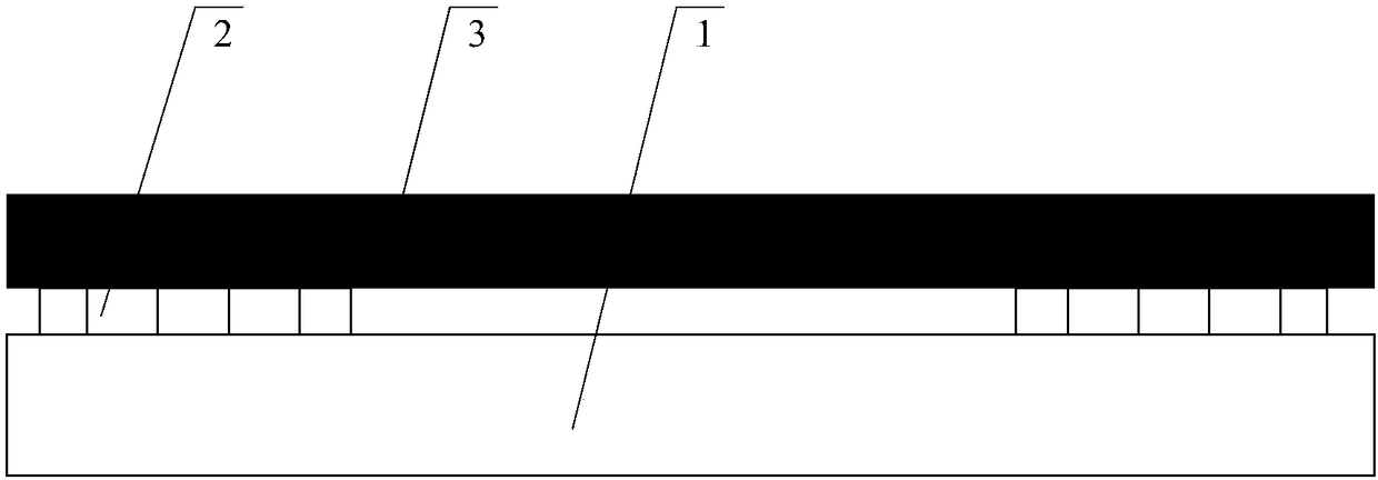
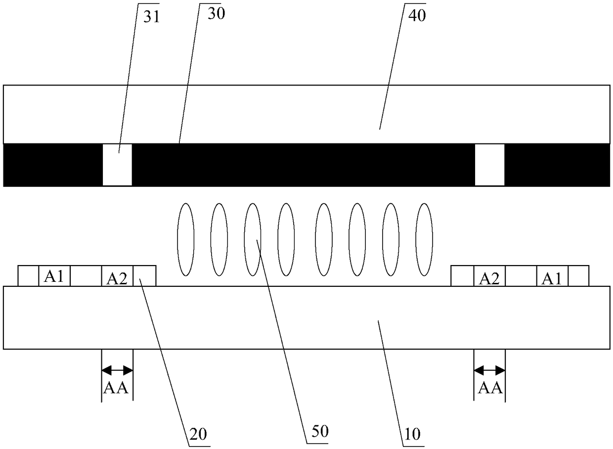
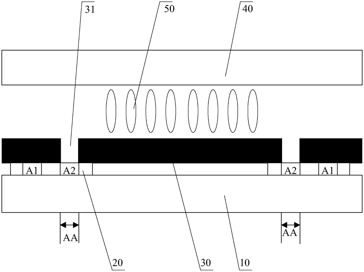
[0057] Embodiments of the present invention provide a display panel, Figure 2A A schematic structural diagram of a display panel provided by an embodiment of the present invention Figure 1 , Figure 2B A second structural schematic diagram of a display panel provided by an embodiment of the present invention, as shown in Figure 2A and Figure 2B As shown, the display panel provided by the embodiment of the present invention includes: a first substrate 10 and a second substrate 40 arranged opposite to each other, a signal line array 20 arranged on the first substrate 10 and a signal line array 20 arranged on the first substrate 10 or the second substrate 40 on the first black matrix layer 30 .
[0058] Specifically, the signal line array includes: clock signal lines and common electrode feedback signal lines; the display panel includes: a first area A1 configured with common electrode feedback signal lines and a second area A2 configured with clock signal lines; The blac...
Embodiment 2
[0095] Based on the inventive concepts of the above embodiments, the embodiments of the present invention further provide a method for manufacturing a display panel, Figure 11 The flow chart of the manufacturing method of the display panel provided by the embodiment of the present invention, such as Figure 11 As shown, the manufacturing method of the display panel provided by the embodiment of the present invention specifically includes the following steps:
[0096] Step 100, providing a first substrate and a second substrate.
[0097] Optionally, the first substrate is a glass substrate, a quartz substrate, or a plastic substrate, which is not limited in this embodiment of the present invention.
[0098] Optionally, the second substrate is a glass substrate, a quartz substrate, or a plastic substrate, which is not limited in this embodiment of the present invention.
[0099] Step 200, forming a signal line array on the first substrate.
[0100] Specifically, the signal l...
Embodiment 3
[0112] Based on the inventive concept of the above embodiments, an embodiment of the present invention further provides a display device, including: a display panel.
[0113] The display panel is the display panel provided in the first embodiment, and its implementation principle and implementation effect are similar, and details are not repeated here.
[0114] It should be noted that the display device may be a Liquid Crystal Display (LCD) device, electronic paper, an Organic Light-Emitting Diode (OLED) device, a mobile phone, a tablet computer, a TV, a monitor, a notebook Computers, digital photo frames, navigators and other products or components with display functions.
[0115] The following points need to be noted:
[0116] The drawings of the embodiments of the present invention only relate to the structures involved in the embodiments of the present invention, and other structures may refer to general designs.
[0117] In the drawings used to describe embodiments of t...
PUM
 Abstract
Description
Claims
Application Information
 - R&D
- Intellectual Property
- Life Sciences
- Materials
- Tech Scout
- Unparalleled Data Quality
- Higher Quality Content
- 60% Fewer Hallucinations
Browse by: Latest US Patents, China's latest patents, Technical Efficacy Thesaurus, Application Domain, Technology Topic, Popular Technical Reports.
© 2025 PatSnap. All rights reserved.Legal|Privacy policy|Modern Slavery Act Transparency Statement|Sitemap|About US| Contact US: help@patsnap.com