Interconnection structure and manufacturing method thereof

A technology of interconnection structure and manufacturing method, applied in semiconductor/solid-state device manufacturing, electrical components, electric solid-state devices, etc., to achieve the effect of maintaining low resistance value and low resistance capacitance delay, preventing circuit bridging defects, and large cross-sectional area

Active Publication Date: 2018-08-14
MACRONIX INT CO LTD
View PDF10 Cites 1 Cited by
  • Summary
  • Abstract
  • Description
  • Claims
  • Application Information

AI Technical Summary

Problems solved by technology

In this way, two adjacent upper layer conductive elements will generate a bridging path (bridging path) through the exposed lower layer conductive element, thereby causing a circuit bridging (circuit bridging) defect

Method used


Image

  • Interconnection structure and manufacturing method thereof
  • Interconnection structure and manufacturing method thereof
  • Interconnection structure and manufacturing method thereof

Examples


Embodiment Construction

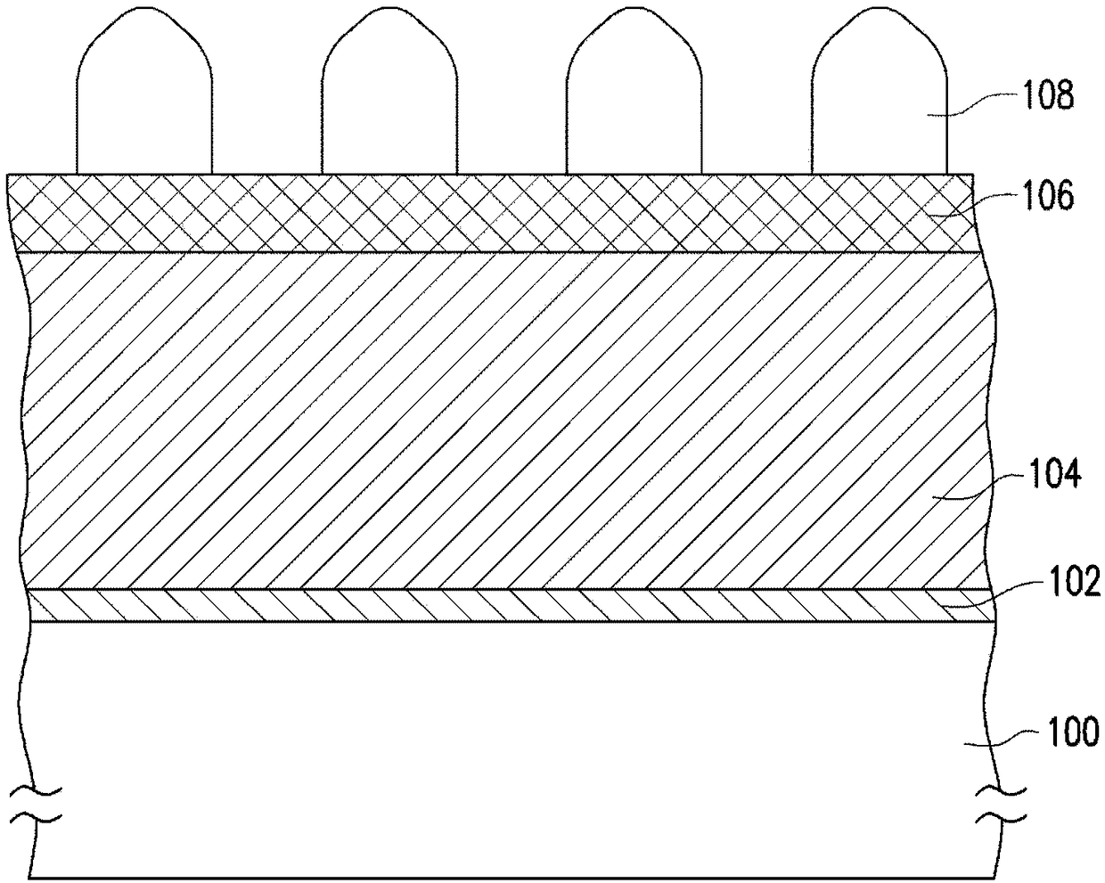
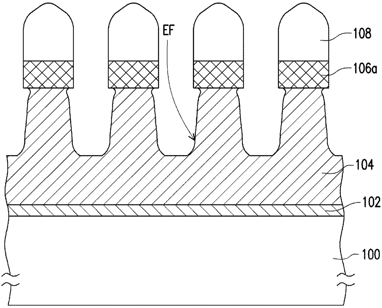
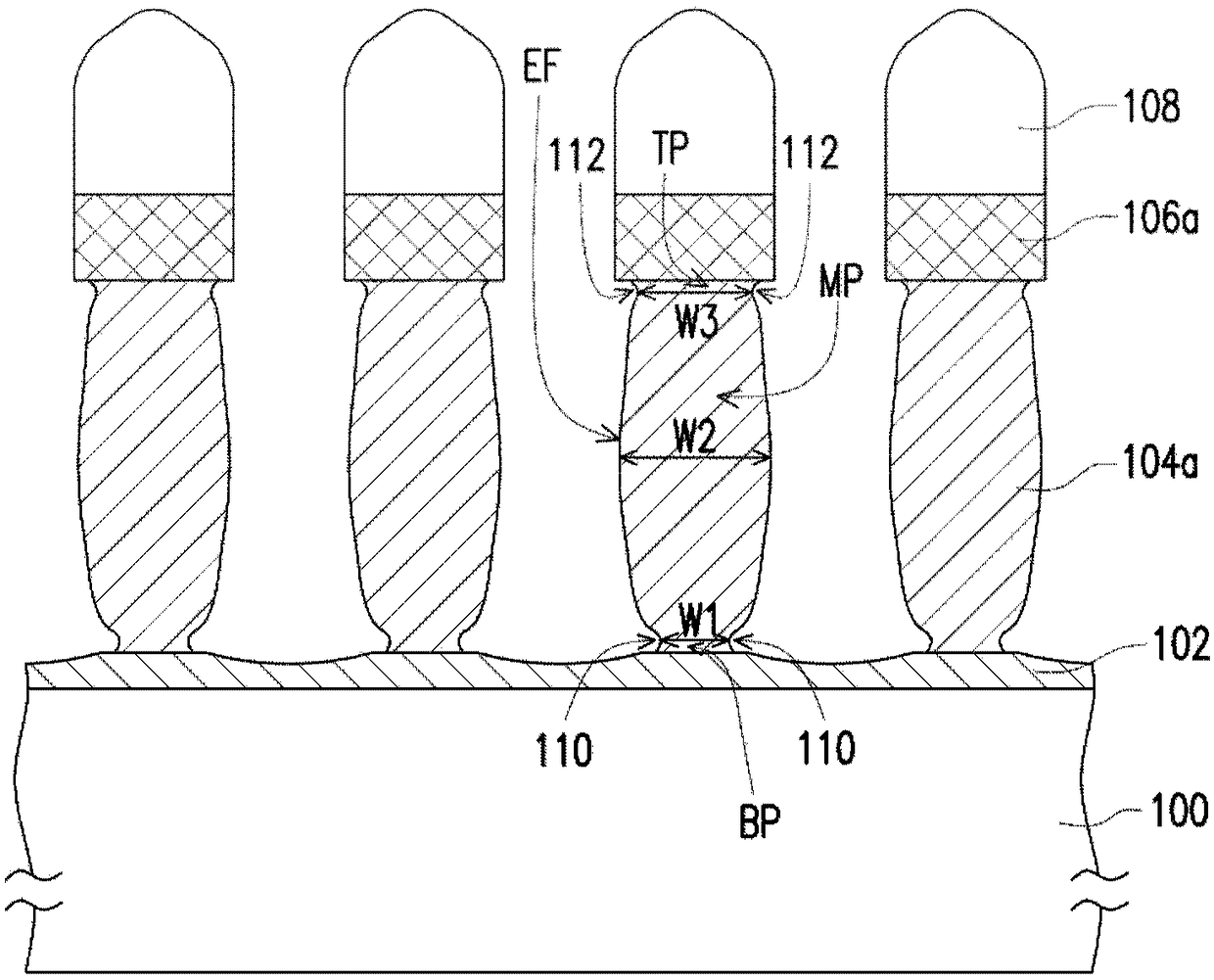
[0035] Figure 1A to Figure 1E It is a sectional view of the manufacturing process of the interconnection structure according to an embodiment of the present invention.

[0036] First, please refer to Figure 1A , providing a substrate 100. The substrate 100 can be a single-layer substrate or a multi-layer substrate, and other film layers (not shown), conductive elements (not shown) or semiconductor elements (not shown) can be formed thereon.

[0037] Next, a barrier material layer 102 can be optionally formed on the substrate 100 . The material of the barrier material layer 102 is, for example, Ti, TiN, Ta, TaN or a combination thereof. The barrier material layer 102 is formed by, for example, physical vapor deposition or chemical vapor deposition.

[0038] Then, a conductive pattern material layer 104 is formed on the barrier material layer 102 . The material of the conductive pattern material layer 104 is, for example, AlCu, Al or W. The method for forming the conducti...


PUM


Abstract

An interconnection structure comprises a substrate and a conductive pattern, wherein the conductive pattern comprises a bottom part, the bottom part of the conductive pattern is arranged on a substrate, and the conductive pattern is provided with gaps in two side walls of the bottom part.

Description

technical field [0001] The present invention relates to a conductive structure and its manufacturing method, and in particular to an interconnection structure and its manufacturing method. Background technique [0002] With the development of the semiconductor industry, when the integration of integrated circuits increases and the surface of the chip cannot provide enough area to make the required interconnection structure, multi-layer interconnection structure design has gradually become a must for many integrated circuits. way of design. [0003] As the semiconductor device shrinks gradually, the overlay window between the upper layer conductive device and the lower layer conductive device below it in the multilayer interconnection structure will also become smaller, so misalignment is prone to occur. When misalignment occurs between the upper layer conductive element and the underlying lower layer conductive element in the multilayer interconnection structure, the upper ...

Claims


Application Information

Patent Timeline
Patent Type & Authority Applications(China)
IPC IPC(8): H01L23/528H01L21/768
CPCH01L21/76838H01L23/5283
Inventor 李鸿志黄旻暄
Owner MACRONIX INT CO LTD
Why Eureka
Try Eureka