Prism total reflection double-lens common-chip module
A chip module and total reflection technology, applied in the field of optical imaging, can solve the problems of damage, high production cost, complicated process, etc., and achieve the effect of reducing imaging error and process cost
- Summary
- Abstract
- Description
- Claims
- Application Information
AI Technical Summary
Problems solved by technology
Method used
Image
Examples
Embodiment Construction
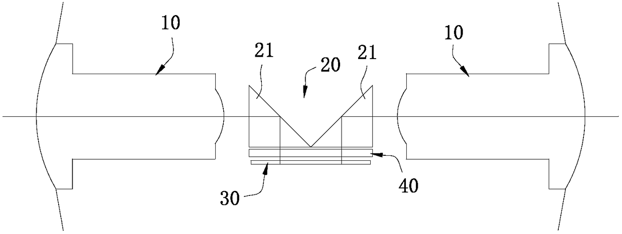
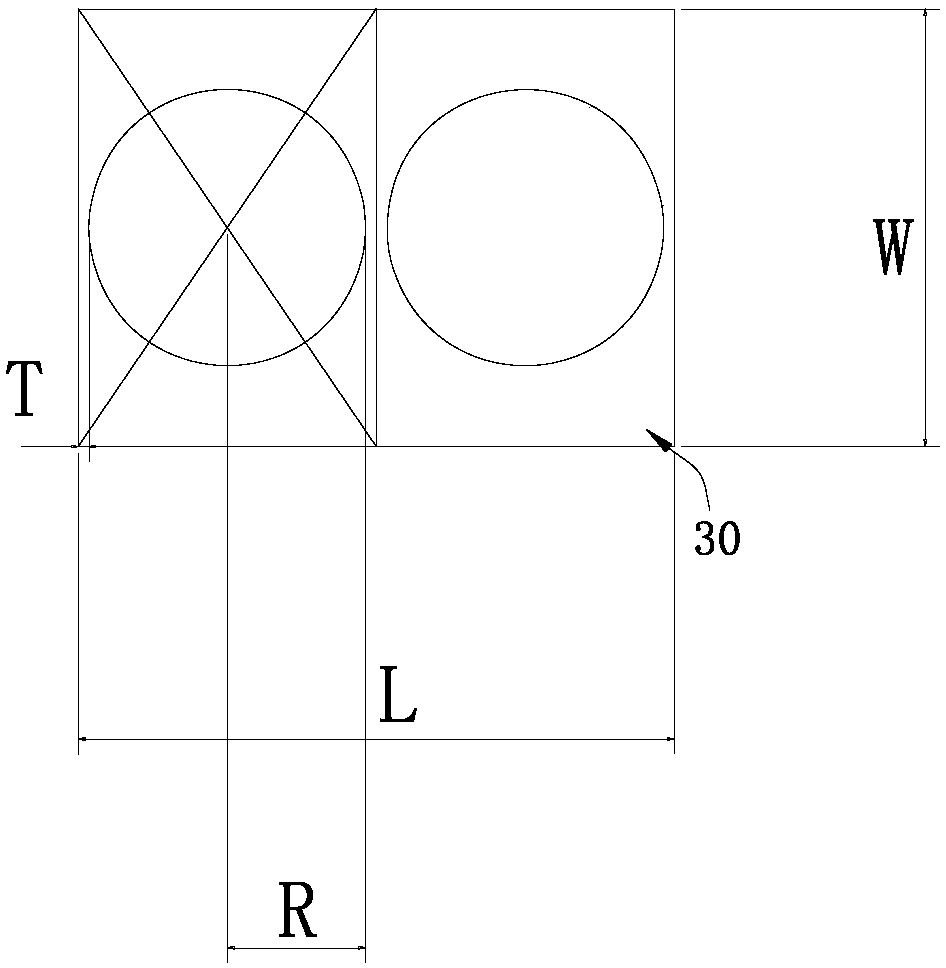
[0022] refer to Figure 1 to Figure 4 , a prism total reflection dual-lens common-chip module of the present invention, comprising two sets of lens assemblies 10 symmetrically distributed left and right and with coincident optical axes, a triangular prism group 20 arranged between the two groups of lens assemblies 10, and a triangular prism group 20 arranged below image sensor 30.
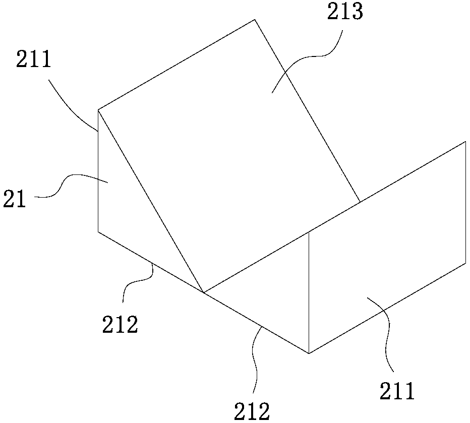
[0023] Wherein, the triangular prism group 20 is composed of two isosceles right-angled triangular prisms 21 symmetrically arranged. The isosceles right-angled triangular prism 21 has an incident surface 211, an outgoing surface 212 and a total reflection surface 213. The incident surface 211 and the outgoing surface 212 are perpendicular to each other. The incident surface 211 of the right-angled triangular prism 21 is in the vertical direction and faces the two left and right lens assemblies 10. The incident surface 211 of the right-angled prism 21 faces the lens assembly 10 on the right side, a...
PUM
 Abstract
Description
Claims
Application Information


