
Manufacturing method of OLED devices

A manufacturing method and device technology, which are applied in semiconductor/solid-state device manufacturing, semiconductor devices, electric solid-state devices, etc., can solve the problem of uneven brightness of OLED display panels, and achieve the effect of preventing the problem of uneven brightness.

Active Publication Date: 2018-08-17
SHENZHEN CHINA STAR OPTOELECTRONICS SEMICON DISPLAY TECH CO LTD
View PDF2 Cites 7 Cited by
  • Summary
  • Abstract
  • Description
  • Claims
  • Application Information

AI Technical Summary

Problems solved by technology

[0005] The purpose of the present invention is to provide a method for manufacturing an OLED device, which can effectively prevent the IR Drop of the OLED device, thereby improving the problem of uneven brightness of the OLED display panel

Method used


Image

  • Manufacturing method of OLED devices
  • Manufacturing method of OLED devices
  • Manufacturing method of OLED devices

Examples


Embodiment Construction

[0031] In order to further illustrate the technical means adopted by the present invention and its effects, the following describes in detail in conjunction with preferred embodiments of the present invention and accompanying drawings.

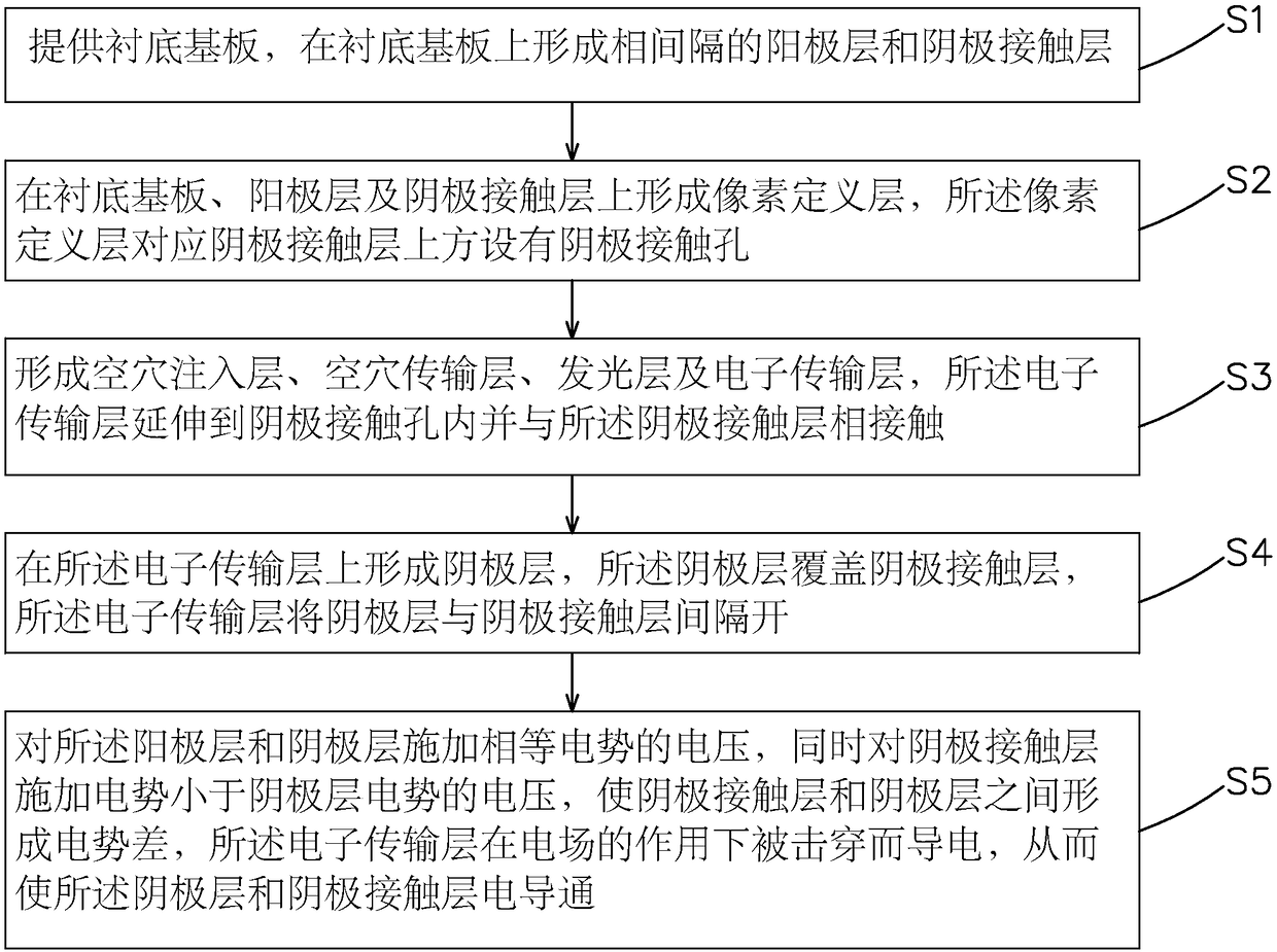
[0032] see figure 1 , the invention provides a kind of fabrication method of OLED device, comprises the following steps:

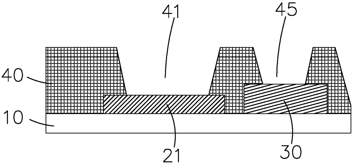
[0033] Step S1, such as figure 2 As shown, a base substrate 10 is provided on which an anode layer 21 and a cathode contact layer 30 are formed spaced apart.

[0034] Specifically, the base substrate 10 is a glass substrate.

[0035] Specifically, in the step S1, the distance between the anode layer 21 and the cathode contact layer 30 is 10 μm-20 μm, and they are not connected to each other.

[0036] Specifically, the materials of the anode layer 21 and the cathode contact layer 30 are hydrophilic conductive materials.

[0037] Step S2, such as image 3 As shown, a pixel definition layer 40 is formed on the base subs...


PUM


Abstract

The invention provides a manufacturing method of OLED (Organic Light Emitting Diodes) devices. The manufacturing method of OLED devices includes the steps: setting a cathode contact layer which is partitioned from an anode layer on a substrate, and setting a cathode contact hole, on a pixel definition layer, corresponding to the upward side of the cathode contact layer, wherein during the manufacturing process, an electron transmission layer extends into the cathode contact hole from a pixel opening to separate a cathode layer from the cathode contact layer; before the device works normally, for electric conduction between the cathode contact layer and the cathode layer, applying positive voltage with equal potential to the cathode layer and the anode layer, and at the same time applying avoltage less than the potential of the cathode layer to the cathode contact layer to enable the potential difference to be formed between the cathode contact layer and the cathode layer, wherein theelectron transmission layer is broken down under the effect of an electric field so as to be conducted, so as to realize electric conduction of the cathode layer and the cathode contact layer; and when an OLED device is working, the cathode contact hole layer can directly provide voltage and current compensation for the cathode layer so as to prevent a display panel of the OLED device encounteringa large area of voltage drop to cause non-uniform brightness.

Description

technical field [0001] The invention relates to the field of display technology, in particular to a method for manufacturing an OLED device. Background technique [0002] Organic Light Emitting Diodes (Organic Light Emitting Diodes, OLED) is a new type of current-mode semiconductor light-emitting device, which is a kind of autonomous light-emitting technology by controlling the injection and recombination of charge carriers in the device to excite organic materials to emit light. Compared with passive luminescent liquid crystal display (Liquid Crystal Display, LCD), self-luminous OLED display has the advantages of fast response, high contrast, wide viewing angle, etc., and it is easy to realize flexible display. It is generally optimistic in the industry, and the industry agrees that OLED display It is very likely to become the mainstream product of the next generation of display technology. [0003] Active-matrix organic light emitting diodes (Active-matrix organic light e...

Claims


Application Information

Patent Timeline
Patent Type & Authority Applications(China)
IPC IPC(8): H01L51/56
CPCH10K71/00H10K59/80522H10K59/122H10K50/16
Inventor 邴一飞
Owner SHENZHEN CHINA STAR OPTOELECTRONICS SEMICON DISPLAY TECH CO LTD
Learn More