Quick heat dissipation PCB
A fast, heat sink technology, applied in the direction of circuit heat devices, printed circuit components, electrical components, etc., can solve the problems of increased heat flux density, increased power consumption of a single component, etc., to improve heat dissipation performance, increase heat dissipation speed, compact effect
- Summary
- Abstract
- Description
- Claims
- Application Information
AI Technical Summary
Problems solved by technology
Method used
Image
Examples
Embodiment 1
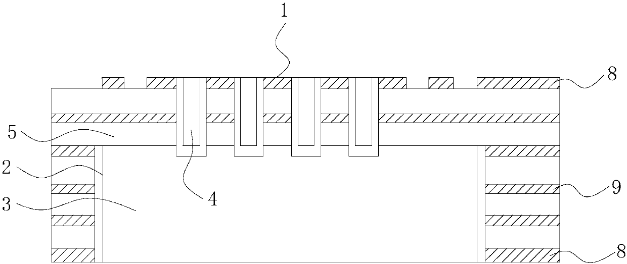
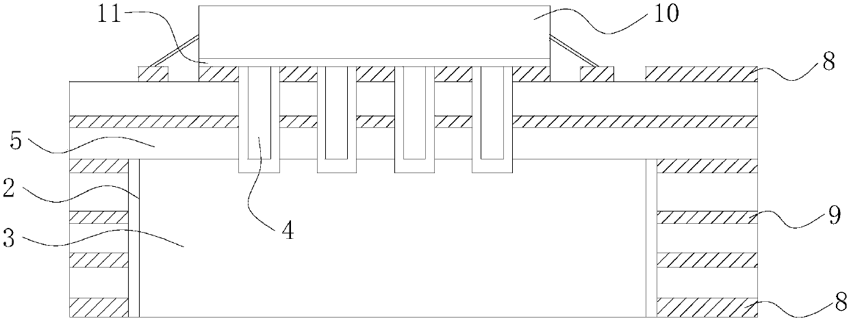
[0057] like figure 1 and 2 As shown, a rapid heat dissipation PCB, the surface of the PCB is designed with a heat source area 1 for installing a heating element 10, the PCB is provided with a heat dissipation slot 2 corresponding to the heat source area 1, and the heat dissipation slot 2 is located on the PCB away from all the On one side of the heat source area 1, a metal block 3 is arranged in the heat dissipation groove 2, and the PCB is also provided with at least one metallized hole 4 corresponding to the heat source area 1, and one end of the metallized hole 4 is connected to the The heat source area 1 is connected, and the other end of the metallized hole 4 is connected to the metal block 3 .
[0058] In this embodiment, the heating element 10 is a high-power component, and the heat source area 1 is the PCB surface covered by the heating element 10 when it is connected to the PCB. The heating element 10 is fixed on the heat source area 1 of the PCB by surface mount te...
Embodiment 2
[0066] The difference between this embodiment and the first embodiment is that:
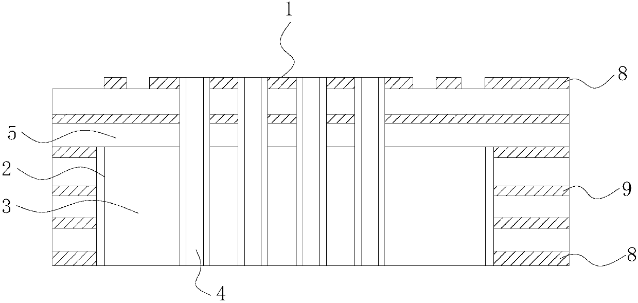
[0067] like image 3 and 4 As shown, the metallized hole 4 is a through hole, and one end of the metallized hole 4 away from the heat source region 1 penetrates the metal block 3 . Under this structure, the heat of the heating element 10 is dissipated simultaneously through two branches, and the first branch is that the heat of the heating element 10 is transferred to the upper part of the metal block 3 through the metallized hole 4 surface, and then the heat is transferred from the upper surface to the lower surface through the metal block 3 to realize the external dissipation of heat; the second branch is that the heat of the heating element 10 is directly transferred through the metallized hole 4 to the The lower surface of the metal block 3 then realizes the external dissipation of heat.
Embodiment 3
[0069] The difference between this embodiment and the first embodiment is that:
[0070] like Figure 5 and 6 As shown, the PCB is also provided with a number of peripheral vias 6, the peripheral vias 6 are located outside the heat dissipation slot 2, and the peripheral vias 6 have metallized sidewalls penetrating the Through holes of the PCB, the peripheral through holes 6 are not in direct contact with the heat sink 2 . Specifically, the peripheral vias 6 not only realize the electrical conduction between the circuit layers, but also realize the transfer of the heat of the inner circuit layer 9 to the surface of the PCB.
PUM
 Abstract
Description
Claims
Application Information


