PNP transistor structure resistant to total dose irradiation

An anti-total dose, transistor technology, applied in the direction of transistors, semiconductor devices, electrical components, etc., can solve the problem of unstable reference output voltage, and achieve the effect of eliminating the effect of total dose radiation

Active Publication Date: 2018-08-24
XIAN MICROELECTRONICS TECH INST
View PDF3 Cites 8 Cited by
  • Summary
  • Abstract
  • Description
  • Claims
  • Application Information

AI Technical Summary

Problems solved by technology

Since the radiation-induced excess electron concentration under the field oxygen layer 3 depends on the cumulative radiation dose, the I/V character

Method used


Image

  • PNP transistor structure resistant to total dose irradiation
  • PNP transistor structure resistant to total dose irradiation
  • PNP transistor structure resistant to total dose irradiation

Examples


Embodiment Construction

[0026] The present invention will be further described in detail below in conjunction with specific embodiments, which are explanations of the present invention rather than limitations.

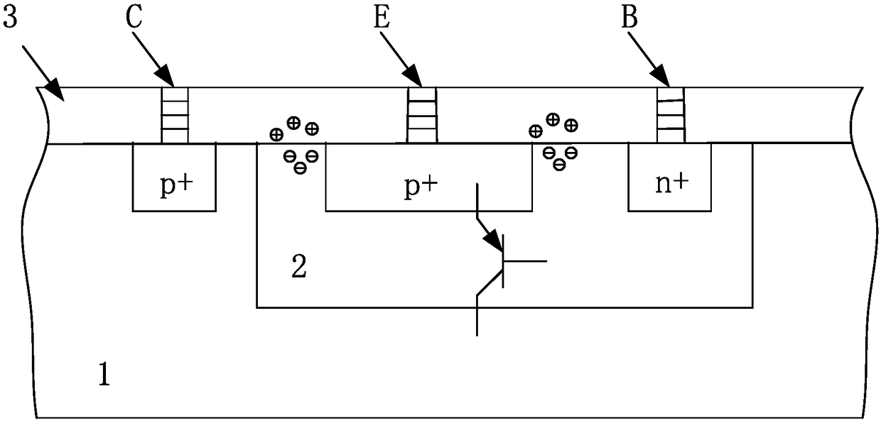
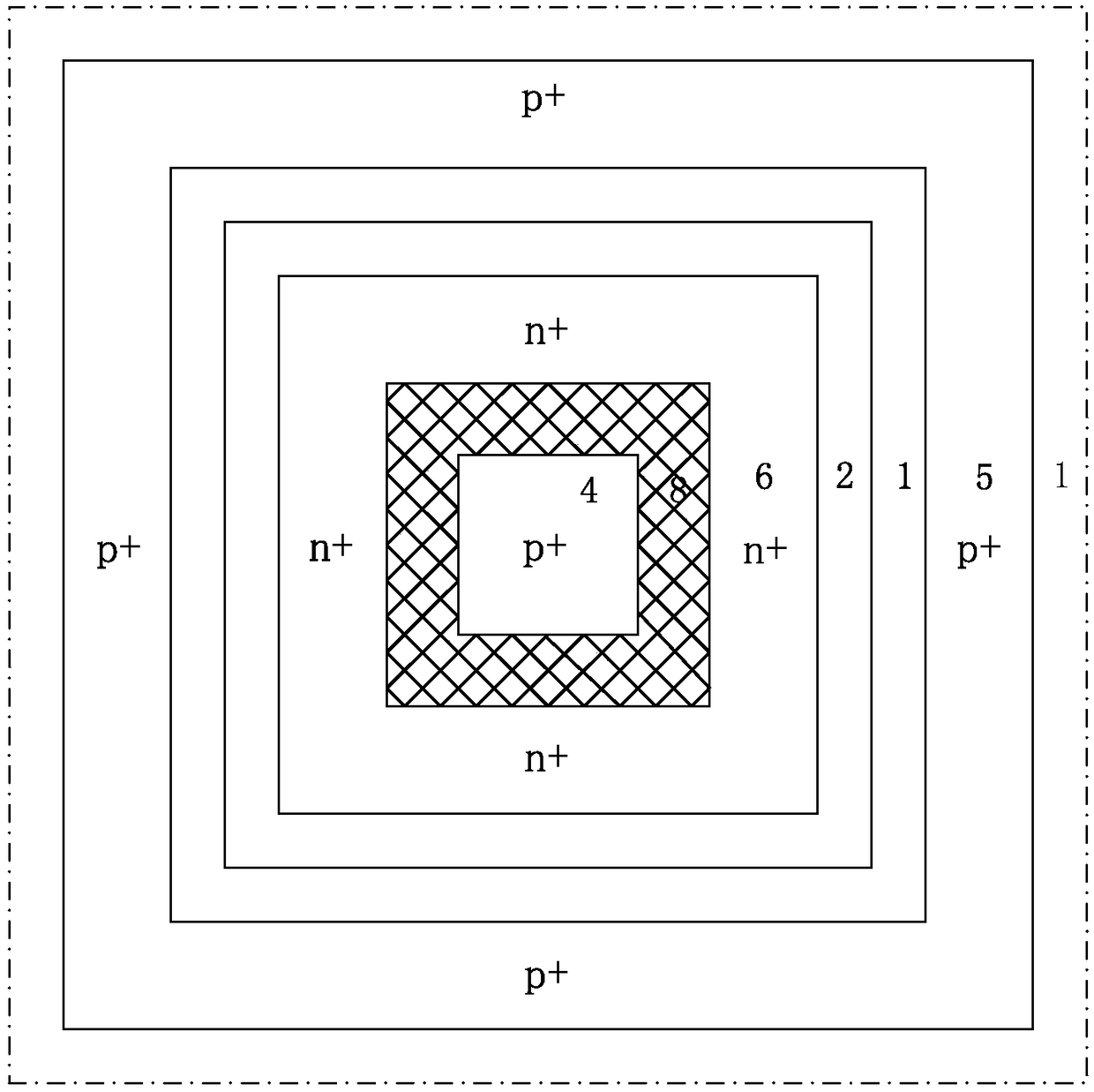
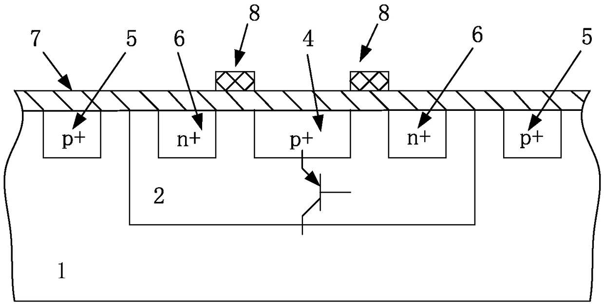
[0027] The invention provides an anti-total dose radiation PNP transistor structure, which is a reinforced structure of a PNP transistor, which is based on a deep submicron CMOS process and adopts a commercial process to suppress the total dose effect of ionizing radiation at a small cost. The performance degradation of PNP transistors improves the ability of CMOS bandgap references to resist the effects of total dose radiation. The annular polysilicon 8 arranged around the first p+ region 4 is adopted, thereby completely avoiding the p-n+ junction formed by the thick field oxygen, and eliminating the total dose radiation effect of the conventional PNP transistor structure.

[0028] Such as figure 2 with image 3 As shown, the specific present invention includes a first p+ region 4, an n+ ...


PUM


Abstract

The invention discloses a PNP transistor structure resistant to total dose irradiation. The PNP transistor structure comprises a p-type substrate and an n-well arranged in the p-type substrate. A second p+ region spaced from the n-well is arranged in the p-type substrate. A first p+ region and an n+ injection region are arranged in the n-well at an interval. An annular polycrystalline silicon gridis arranged outside the first p+ region in a surrounding mode. Compared with a PNP transistor prepared through the conventional CMOS (complementary metal oxide semiconductor) process, the annular polycrystalline silicon grid is adopted to surround the first p+ region, so that the formation of p/n+ junctions caused by the thick-field oxygen in the prior art is completely avoided. The total dose radiation effect is eliminated. As a result, the total dose irradiation resistance of the CMOS band gap reference reaches 300 krad (Si) under the dosage rate of 50 rad(Si)/s.

Description

technical field [0001] The invention relates to the field of radiation reinforcement against total dose radiation effect, in particular to a PNP transistor structure against total dose radiation. Background technique [0002] When the device is continuously exposed to ionizing radiation (such as gamma rays and X-rays, etc.), the total dose radiation effect will occur. Under the condition of total dose radiation, the ionization in the silica medium produces a certain number of electron-hole pairs. When there is an electric field, oxide trap charges and interface state charges are accumulated in silicon dioxide, thereby affecting the performance of the device. [0003] CMOS bandgap reference is a widely used module in CMOS analog integrated circuits. Its performance depends on the pn junction characteristics in the forward biased state. Bandgap Reference Circuits As feature sizes in CMOS technology get smaller, circuits become more sensitive to total dose radiation. The ma...

Claims


Application Information

Patent Timeline
IPC IPC(8): H01L29/73H01L29/423H01L29/06
CPCH01L29/0684H01L29/423H01L29/73
Inventor 刘智姜洪雨葛梅梁希
Owner XIAN MICROELECTRONICS TECH INST
Why Eureka
Try Eureka