
Eureka
For R&D, Eureka makes reading and utilizing patents & technical documents easy.
Eureka AIR
Designed for self-driven R&D workflows. Generate viable solutions, solve complex R&D challenges, empower your innovation with AI.

Eureka Materials
Designed for material experts only. Revolutionize your material R&D, from search, analyze, to developing new materials.

TechResearch
Generate reliable direction feasibility study reports for your R&D in just a few steps.

TechSeek
Discover and master advanced knowledge NOW. Basics, ideas, possibilities, all at once.

TechMind
As an expert in R&D Theories, TechMind can generates customized viable solutions instantly.

TechRisk
Analyze your overall solution with one click, know your potential R&D risks in advance.

TechMonitor
Get weekly tech updates, stay abreast of the latest tech innovations and key insights.
Smear detection device, laser via processing device, and laser via processing method
A detection device, laser drilling technology, applied to measuring devices, fluorescence/phosphorescence, laser welding equipment, etc., can solve the problem that visual inspection takes a long time
- Summary
- Abstract
- Description
- Claims
- Application Information
AI Technical Summary
Problems solved by technology
Method used
Image

Examples
Embodiment Construction
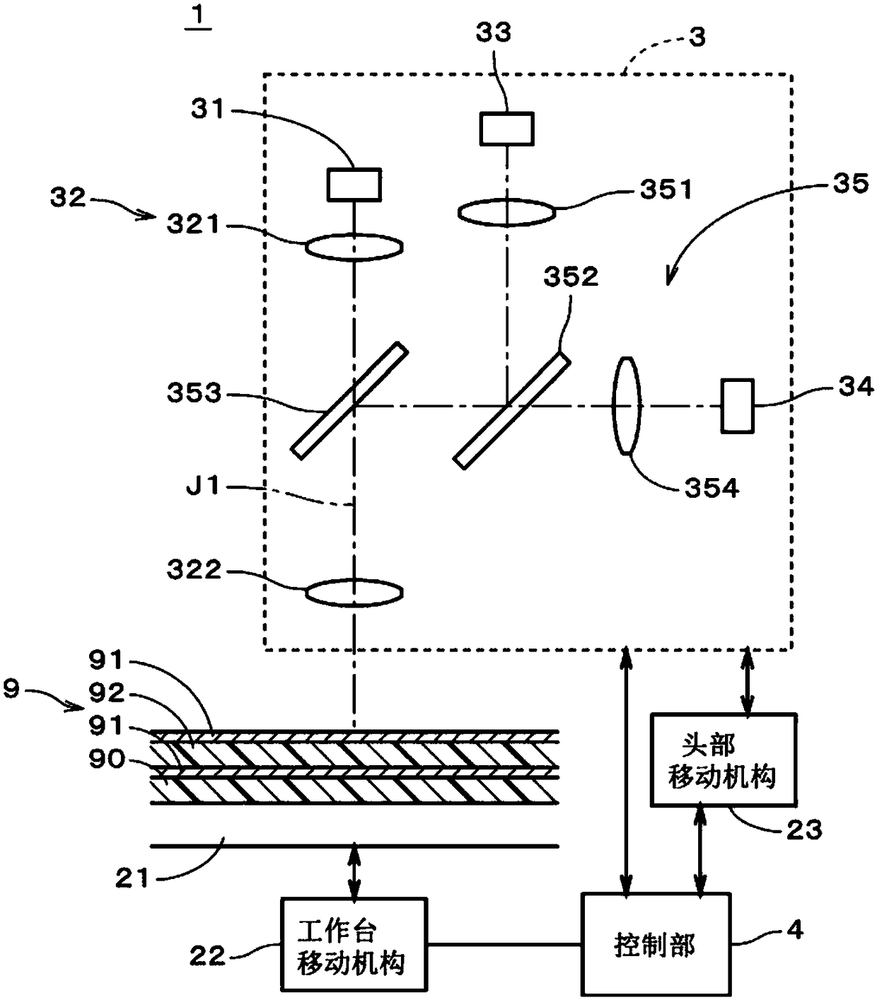
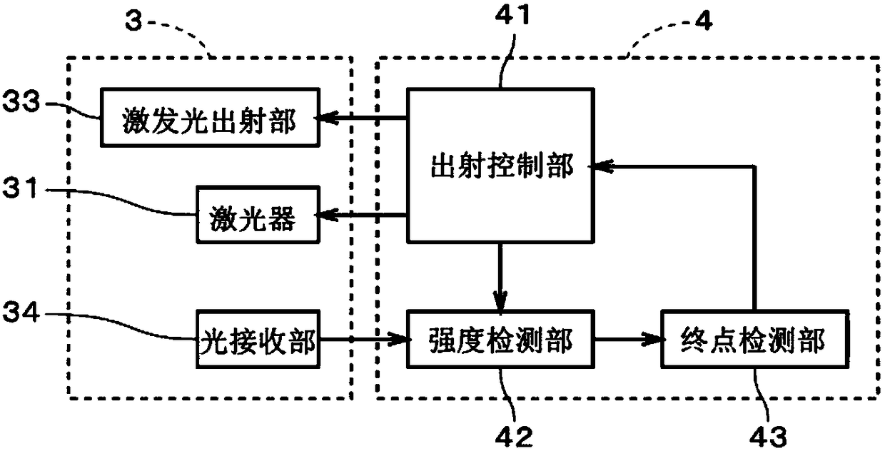
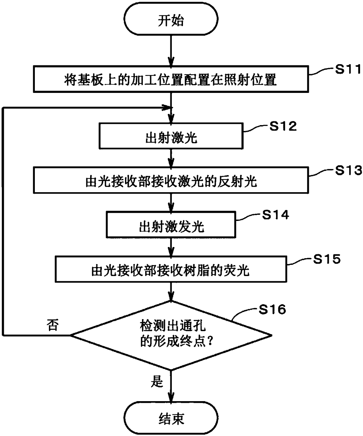
[0023] figure 1 It is a figure which shows the structure of the laser drilling processing apparatus 1 which concerns on one Embodiment of this invention. The laser drilling processing device 1 is used for laser drilling processing when manufacturing the multilayer substrate 9 , that is, using a laser to form through holes on the multilayer substrate 9 in the manufacturing process. The laser drilling process is a part of the connection process in the manufacture of the multilayer substrate 9 . In the multilayer substrate 9 , for example, wiring layers 91 and insulating layers 92 are alternately laminated on a plate-shaped or thin-plate-shaped base material 90 formed of resin. The wiring layer 91 is a wiring pattern formed of a conductive material such as copper. The insulating layer 92 is formed of a resin such as polyimide, and insulates adjacent wiring layers 91 . In the following description, the multilayer substrate 9 in the process of manufacture is simply referred to a...
PUM
 Abstract
Description
Claims
Application Information
 - R&D Engineer
- R&D Manager
- IP Professional
- Industry Leading Data Capabilities
- Powerful AI technology
- Patent DNA Extraction
Browse by: Latest US Patents, China's latest patents, Technical Efficacy Thesaurus, Application Domain, Technology Topic, Popular Technical Reports.
© 2024 PatSnap. All rights reserved.Legal|Privacy policy|Modern Slavery Act Transparency Statement|Sitemap|About US| Contact US: help@patsnap.com