Peeling method and method of manufacturing semiconductor device

Inactive Publication Date: 2008-04-01
SEMICON ENERGY LAB CO LTD
View PDF140 Cites 172 Cited by
  • Summary
  • Abstract
  • Description
  • Claims
  • Application Information

AI Technical Summary

Benefits of technology

[0011]The present invention has been made in view of the above problems. An object of the present invention is therefore to provide a peeling method in which a layer to be peeled is

Problems solved by technology

With respect to a laminate of the first material layer and the second ma

Method used


Image

  • Peeling method and method of manufacturing semiconductor device
  • Peeling method and method of manufacturing semiconductor device
  • Peeling method and method of manufacturing semiconductor device

Examples


embodiment mode 1

[Embodiment Mode 1]

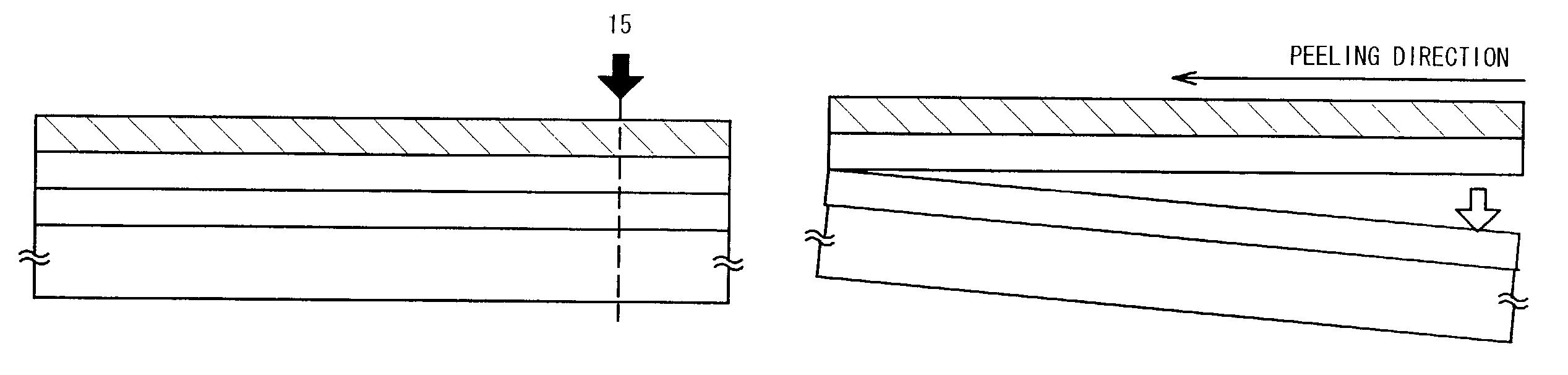
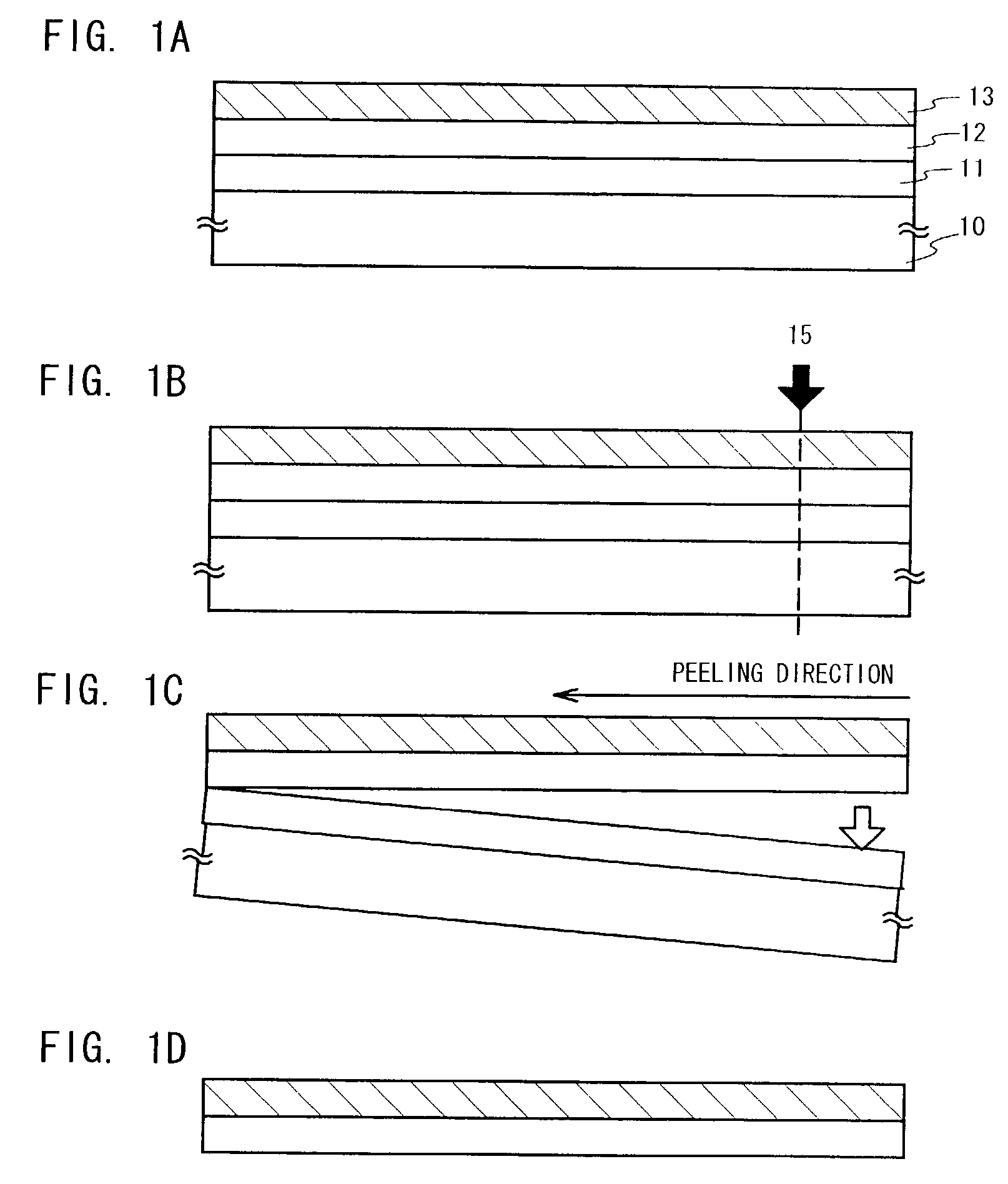
[0076]Hereinafter, a typical peeling order according to the present invention will be briefly described using FIGS. 1A to 1D.

[0077]In FIG. 1A, reference numeral 10 denotes a substrate, 11 denotes a first material layer having tensile stress, 12 denotes a second material layer having compression stress, and 13 denotes a layer to be peeled.

[0078]In FIG. 1A, a glass substrate, a quartz substrate, a ceramic substrate, or the like can be used as the substrate 10. In addition, a silicon substrate, a metallic substrate, or a stainless steel substrate may be alternatively used.

[0079]First, as shown in FIG. 1A, the first material layer 11 is formed on the substrate 10. The first material layer 11 may have compression stress or tensile stress immediately after the formation. It is important that the first material layer is formed from a material with which a trouble such as peeling is not caused by heat treatment or laser light irradiation at the formation of the layer to b...

embodiment mode 2

[Embodiment Mode 2]

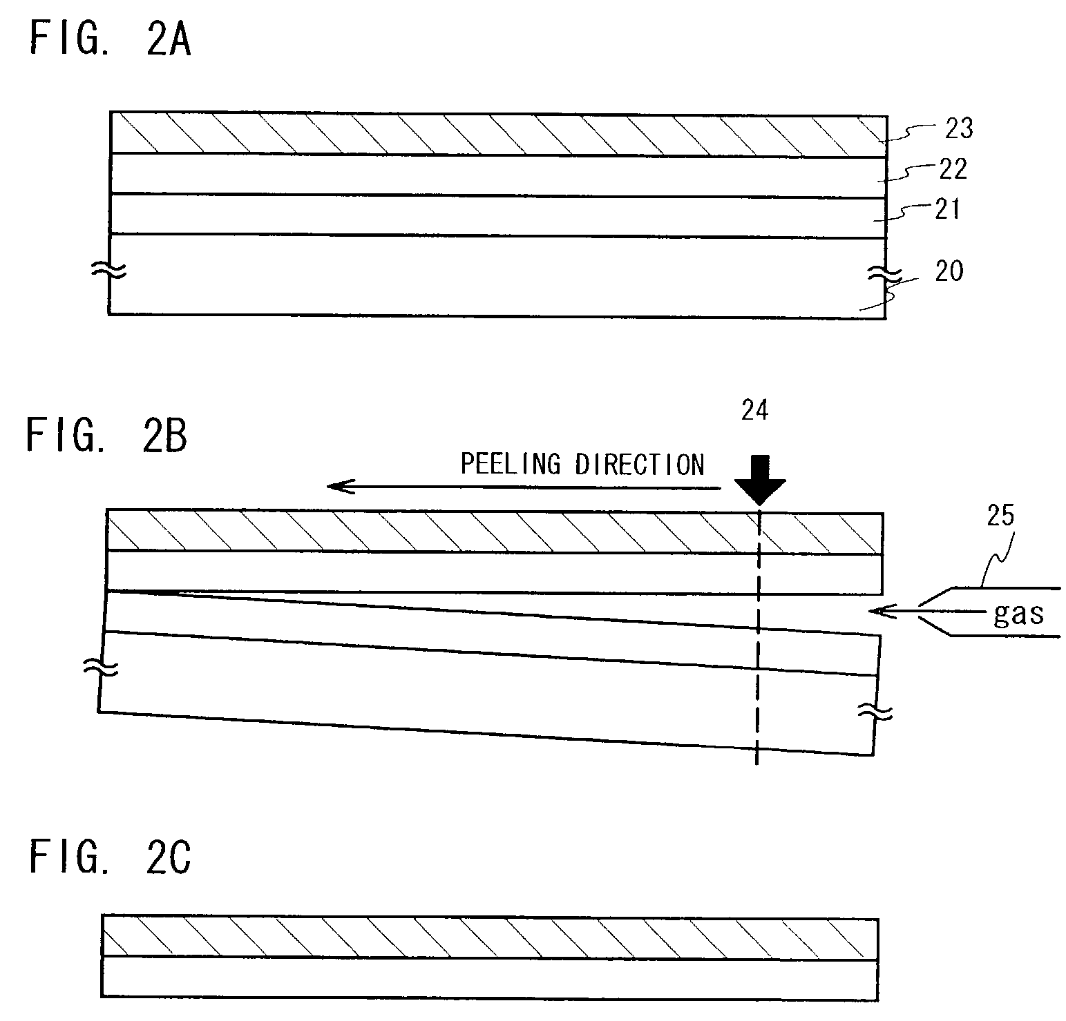
[0094]In this embodiment mode, an example in which a layer to be peeled is peeled while a gas is blown onto an end surface thereof will be briefly described using FIGS. 2A to 2C.

[0095]In FIG. 2A, reference numeral 20 denotes a substrate, 21 denotes a first material layer having tensile stress, 22 denotes a second material layer having compression stress, and 23 denotes a layer to be peeled. Note that FIG. 2A is the same drawing as FIG. 1A and detailed descriptions are omitted here.

[0096]After the state shown in FIG. 2A is obtained by the same order as Embodiment Mode 1, as shown in FIG. 2B, while laser light 24 is irradiated to a portion, a gas is blown at a high pressure from a nozzle 25 to an interface between the first material layer and the second material layer within an end surface of the substrate, thereby conducting peeling in a direction indicated by an arrow in FIG. 2B.

[0097]Here, a wind pressure is used as physical means. However, it is needless to say ...

embodiment mode 3

[Embodiment Mode 3]

[0105]In this embodiment mode, an example in which a pressure is applied to a layer to be peeled by a diamond pen before peeling to partially reduce contact property will be briefly described using FIGS. 3A to 3D.

[0106]In FIG. 3A, reference numeral 30 denotes a substrate, 31 denotes a first material layer having tensile stress, 32 denotes a second material layer having compression stress, and 33 denotes a layer to be peeled. Note that FIG. 3A is the same drawing as FIG. 1A and detailed descriptions are omitted here.

[0107]After the state shown in FIG. 3A is obtained by the same order as Embodiment Mode 1, as shown in FIG. 3B, external force 35 is applied to a pen 34 to scratch the layer to be peeled, thereby partially reducing the contact property between the first material layer 31 and the second material layer 32. The diamond pen is used here. Preferably, a hard needle is vertically pressed and moved under a load.

[0108]Thus, it is important to prepare a portion w...


PUM

PropertyMeasurementUnit
Tensile stressaaaaaaaaaa
Temperatureaaaaaaaaaa
Fractionaaaaaaaaaa

Abstract

There is provided a peeling method capable of preventing a damage to a layer to be peeled. Thus, not only a layer to be peeled having a small area but also a layer to be peeled having a large area can be peeled over the entire surface at a high yield. Processing for partially reducing contact property between a first material layer (11) and a second material layer (12) (laser light irradiation, pressure application, or the like) is performed before peeling, and then peeling is conducted by physical means. Therefore, sufficient separation can be easily conducted in an inner portion of the second material layer (12) or an interface thereof.

Description

BACKGROUND OF THE INVENTION[0001]1. Field of the Invention[0002]The present invention relates to a semiconductor device having a circuit composed of thin film transistors (hereinafter referred to as TFTs) and a manufacturing method thereof. The present invention relates to an electro-optical device which is represented by, for example, a liquid crystal display panel and an electronic device on which such an electro-optical device is mounted as a part.[0003]Note that a semiconductor device in this specification indicates a general device functioning by utilizing semiconductor characteristics, which includes an electro-optical device, a light emitting device, a semiconductor circuit, and an electronic device.[0004]2. Description of the Related Art[0005]In recent years, a technique of constructing a thin film transistor (TFT) using a semiconductor thin film (about several to several hundred nm in thickness) formed on a substrate having an insulating surface has drawn attention. The thi...

Claims


Application Information

Patent Timeline
IPC IPC(8): H01L21/301B32B38/10G02F1/1333B32B7/06B32B43/00H01L21/02H01L21/20H01L21/322H01L21/336H01L21/762H01L21/77H01L21/84H01L27/12H01L27/32H01L29/786H01L51/50H01L51/52H05B33/10
CPCB32B7/06H01L21/76251H01L27/1214H01L27/1266H01L29/66757H01L51/003H01L29/6675H01L29/78663B32B43/006Y10T156/1939B32B2310/0843B32B2457/08B32B2457/14G02F2001/13613H01L21/3221H01L27/3244H01L51/5237H01L51/529Y10S438/977Y10T156/1137Y02E10/549G02F1/13613Y02P70/50H10K59/12H10K71/80H10K50/8426H10K50/87H01L29/786H10K59/122H10K59/123H10K59/124H10K71/00H10K77/111H10K50/84H10K59/1201H10K2102/311G02F1/1368
Inventor TAKAYAMA, TORUMARUYAMA, JUNYAYAMAZAKI, SHUNPEI
Owner SEMICON ENERGY LAB CO LTD
Why Eureka
Try Eureka