Microstrip line slow wave structure

A technology of slow wave structure and microstrip line, which is applied to the circuit components of time-of-flight tubes, and can solve the problems of low interaction efficiency, low coupling impedance, and electromagnetic wave attenuation of traveling wave tube amplifiers.

Active Publication Date: 2018-08-28
UNIV OF ELECTRONICS SCI & TECH OF CHINA
View PDF3 Cites 5 Cited by
  • Summary
  • Abstract
  • Description
  • Claims
  • Application Information

AI Technical Summary

Problems solved by technology

[0005] However, there are also some problems in the microstrip slow-wave structure: the dielectric substrate is placed on the surface of the metal shielding cavity, and the electromagnetic waves transmitted by the microstrip slow-wave structure are quasi-TEM waves, and the electromagnetic waves are mainly concentrated in the dielectric substrate; The electromagnetic field exists in the form of surface waves, and the electromagnetic wave decays exponentially with the distance away from the microstrip line
[0009] It can be seen from the above formula that the coupling impedance is also low due to the weak longitudinal electric field in the conventional microstrip slow-wave structure, which ultimately makes the interaction efficiency of the microstrip planar TWT amplifier low

Method used


Image

  • Microstrip line slow wave structure
  • Microstrip line slow wave structure
  • Microstrip line slow wave structure

Examples


Embodiment Construction

[0023] Specific embodiments of the present invention will be described below in conjunction with the accompanying drawings, so that those skilled in the art can better understand the present invention. It should be noted that in the following description, when detailed descriptions of known functions and designs may dilute the main content of the present invention, these descriptions will be omitted here.

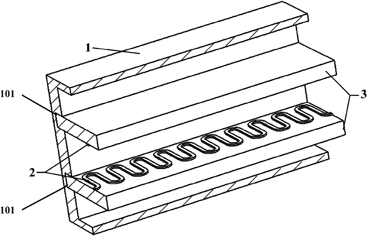
[0024] figure 1 It is a structural schematic diagram of a specific embodiment of the microstrip line slow wave structure of the present invention.

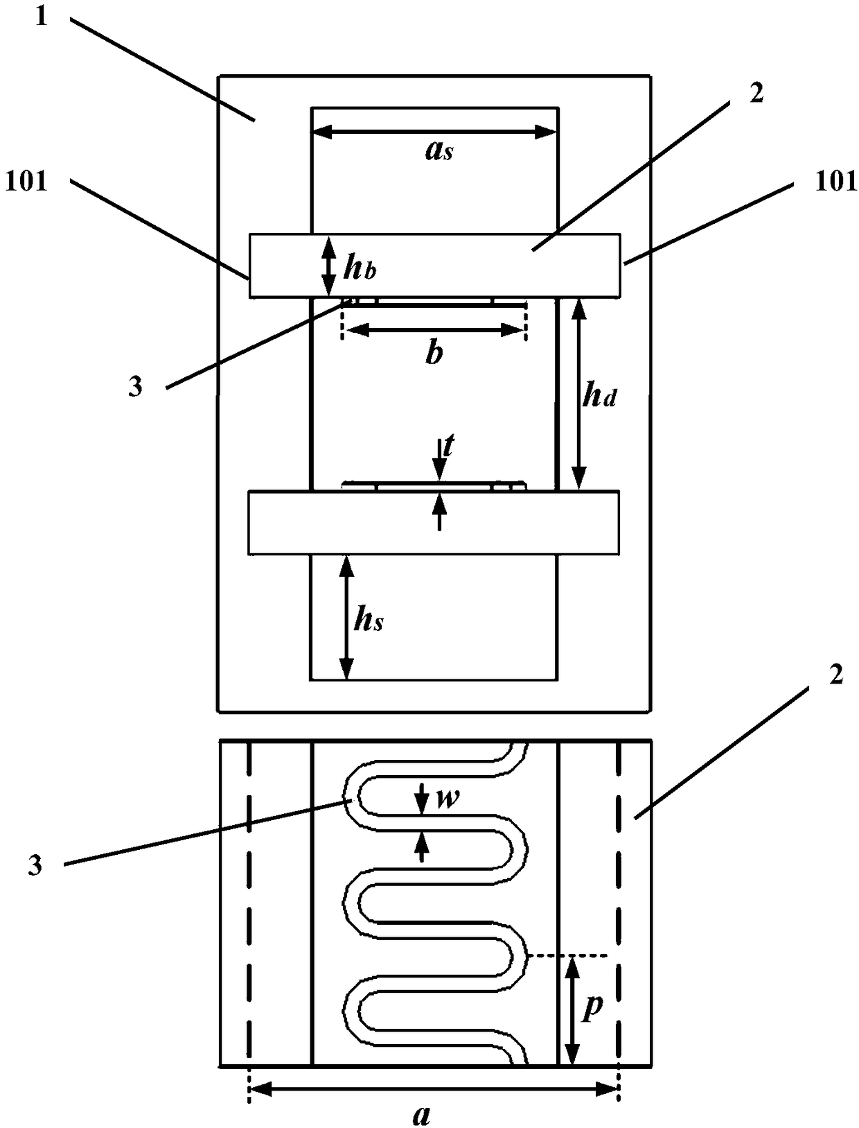
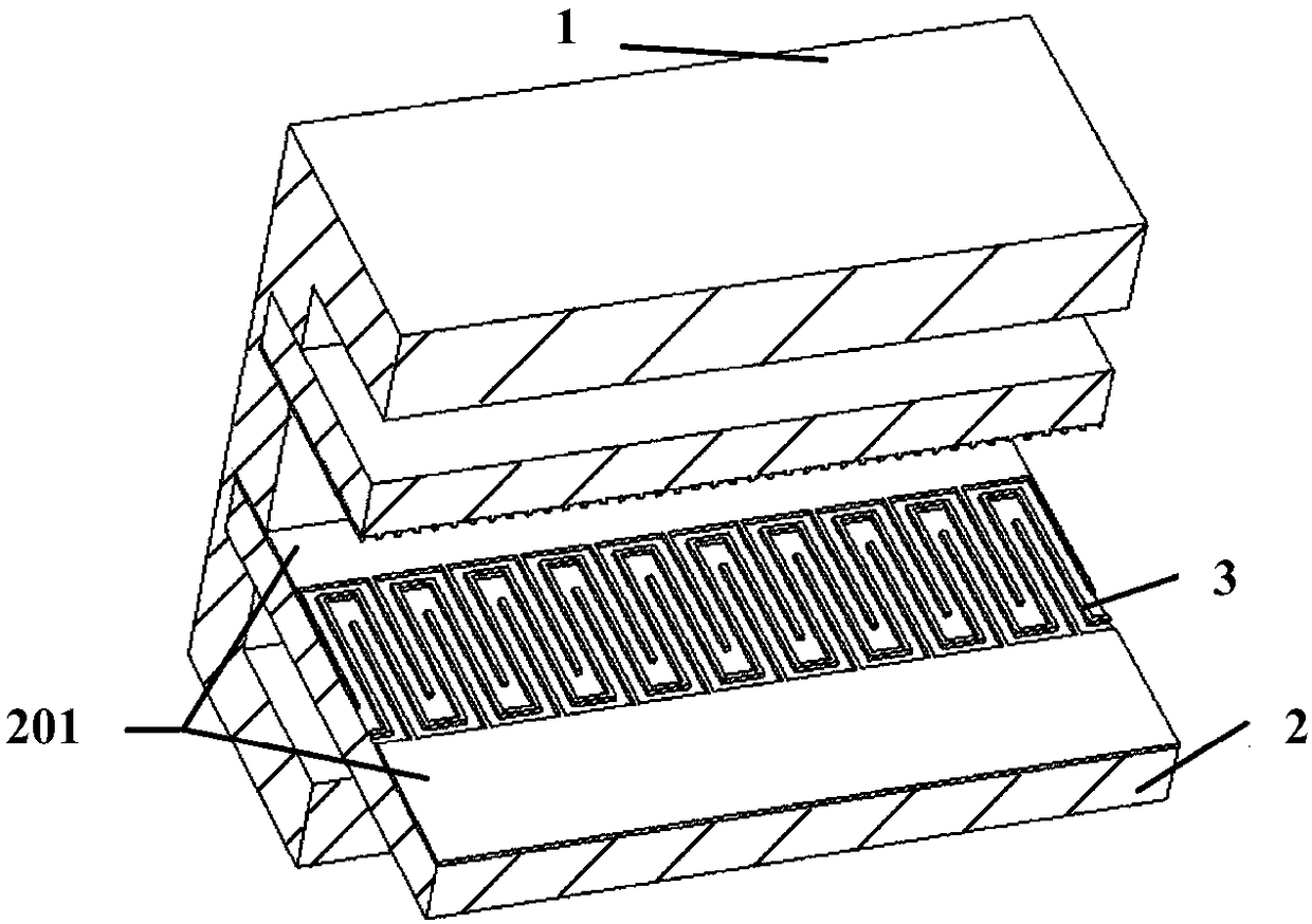
[0025] In this example, if figure 1 As shown, the microstrip slow-wave structure of the present invention includes a vacuum rectangular metal shielding cavity 1 and a dielectric substrate 3 printed with periodic metal meandering microstrip lines 2 on the surface.

[0026] Slots are grooved on both sides of the inner side of the rectangular metal shielding cavity 1 (transmission direction), that is, grooves 101, and the dielec...


PUM


Abstract

The invention discloses a microstrip line slow wave structure. Unlike a conventional microstrip line slow wave structure, a periodic metal meandering microstrip line or a coplanar waveguide is suspended, so that the dielectric substrate with the surface printed with the periodic metal meandering microstrip line or the coplanar waveguide mainly plays a supporting role, the electromagnetic waves aremainly distributed in the vacuum cavities on the upper and lower sides of the dielectric substrate, and the upper side of the periodic metal meandering microstrip line or the coplanar waveguide willhave a strong longitudinal electric field distribution, thereby obtaining a large coupling impedance, and ultimately improving the interaction efficiency of the microstrip line planar traveling wave tube amplifier. Taking the Ka-band N-type periodic metal meander microstrip line slow wave structure as an example, the coupling impedance at 35 GHz is increased by 86.3% by suspending the N-type periodic metal meandering microstrip line.

Description

technical field [0001] The invention belongs to the field of microwave electric vacuum technology, and more specifically relates to a microstrip line slow wave structure in a traveling wave tube amplifier. Background technique [0002] As an important class of microwave and millimeter wave power sources, electric vacuum devices are widely used in communication, guidance, remote sensing and other technical fields. Although electric vacuum devices have the advantages of high power, high gain, high efficiency, high frequency and long life, solid-state power amplifier devices are small in size, light in weight, and can be integrated. , is posing a growing challenge to electric vacuum devices. How to achieve miniaturization and low voltage while ensuring the advantages of electric vacuum devices, so as to better meet the needs of technological development, is an important development direction of microwave electric vacuum devices. [0003] Microwave power modules combine the ad...

Claims


Application Information

Patent Timeline
Patent Type & Authority Applications(China)
IPC IPC(8): H01J23/24
CPCH01J23/24
Inventor 丁冲魏彦玉李倩徐进岳玲娜殷海荣赵国庆王文祥宫玉彬
Owner UNIV OF ELECTRONICS SCI & TECH OF CHINA
Why Eureka
Try Eureka