Micro LED display panel manufacturing method and Micro LED display panel

A technology of a display panel and a manufacturing method, which is applied in the manufacture of semiconductor/solid-state devices, electrical components, and electric solid-state devices, etc., can solve the problem that the upper pixel electrode and the MicroLED upper electrode cannot be properly attached, and the upper pixel electrode and the MicroLED upper electrode cannot be realized. Electrical connection and other issues, to avoid poor connection and improve the effect of the group

Active Publication Date: 2018-09-04
SHENZHEN CHINA STAR OPTOELECTRONICS TECH CO LTD
View PDF5 Cites 17 Cited by
  • Summary
  • Abstract
  • Description
  • Claims
  • Application Information

AI Technical Summary

Problems solved by technology

[0005] In a display panel using a vertical Micro LED, it is necessary to set up an upper pixel electrode and a lower pixel electrode corresponding to the upper and lower electrodes to drive its operation. The upper pixel electrode is fabricated on the packaging substrate, and the lower pixel electrode is fabricated on the driving substrate. Then the packaging substrate and the driving substrate are combined to obtain a Micro LED display panel. At this time, when the packaging substrate and the driving substrate are combined, due to the unevenness above the Micro LED, that is, the height of each Micro LED is not exactly the same. Some upper pixel electrodes and the upper electrode of the Micro LED cannot be properly bonded, resulting in the problem that the upper pixel electrode and the upper electrode of the Micro LED cannot be electrically connected

Method used


Image

  • Micro LED display panel manufacturing method and Micro LED display panel
  • Micro LED display panel manufacturing method and Micro LED display panel
  • Micro LED display panel manufacturing method and Micro LED display panel

Examples


Embodiment Construction

[0028] In order to further illustrate the technical means adopted by the present invention and its effects, the following describes in detail in conjunction with preferred embodiments of the present invention and accompanying drawings.

[0029] see Figure 4 , the present invention provides a method for manufacturing a Micro LED display panel, comprising the following steps:

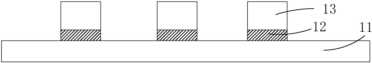
[0030] Step S1, please refer to figure 1 , providing a driving substrate 11, forming a plurality of lower pixel electrodes 12 arranged in an array on the driving substrate 11, and forming a vertical Micro LED 13 on each lower pixel electrode 12, and each lower pixel electrode 12 is connected with the Corresponding to the electrical connection of the lower electrode of Micro LED13;

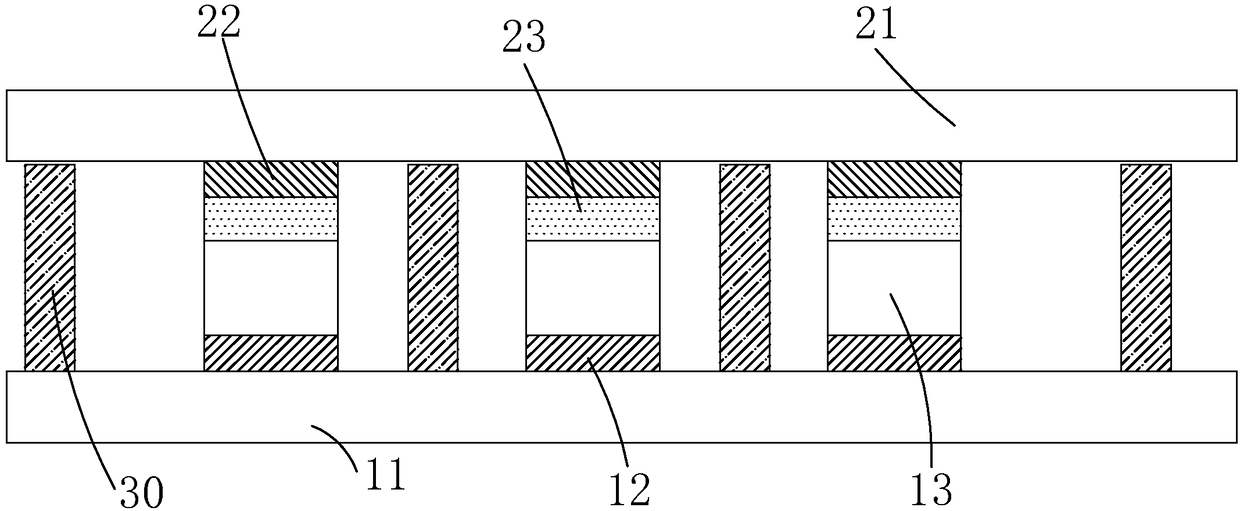
[0031] Step S2, please refer to figure 2 , providing a packaging substrate 21, forming a plurality of upper pixel electrodes 22 arranged in an array on the packaging substrate 21, and forming an elastic conductive layer 2...


PUM


Abstract

The invention provides a Micro LED display panel manufacturing method and a Micro LED display panel. The Micro LED display panel manufacturing method is characterized in that, by forming elastic conductive layers on upper pixel electrodes on a package substrate, when the package substrate is paired with a driving substrate, electrical connection between the upper pixel electrodes and upper electrodes of Micro LEDs is realized through the elastic conductive layers; and height difference between the Micro LEDs can be filled by utilizing elasticity of the elastic conductive layers, thereby preventing poor connection between the upper pixel electrodes and the upper electrodes of the Micro LEDs, and improving pairing effect of the Micro LED display panel and process yield of the Micro LED display panel.

Description

technical field [0001] The present invention relates to the field of display technology, in particular to a method for manufacturing a Micro LED display panel and a Micro LED display panel. Background technique [0002] With the rapid development of wearable display devices, micro light emitting diode (Micro LED, uLED) technology has emerged. Micro LED technology, that is, LED miniaturization and matrix technology, refers to a high-density micro-sized LED array integrated on a chip. The power consumption of Micro LED is much smaller than that of Liquid Crystal Display (LCD), and it is self-illuminating like Organic Light-Emitting Diode (OLED), which can reduce the distance between pixels from the millimeter level to the micron level , the color saturation is close to that of OLED, so many manufacturers regard Micro LED as the next-generation display technology. [0003] The existing technology uses the Micro Transfer Print (Micro Transfer Print) method to make Micro LED ar...

Claims


Application Information

Patent Timeline
Patent Type & Authority Applications(China)
IPC IPC(8): H01L21/77H01L27/32
CPCH01L21/77H10K59/12
Inventor 陈黎暄
Owner SHENZHEN CHINA STAR OPTOELECTRONICS TECH CO LTD
Why Eureka
Try Eureka