Charged-particle beam lens

a particle beam and beam lens technology, applied in the field of charged particle beam optical system, can solve problems such as dielectric breakdown and discharge, and achieve the effects of suppressing discharge generation, increasing resistance, and poor connection

Inactive Publication Date: 2014-04-29
CANON KK
View PDF11 Cites 3 Cited by
  • Summary
  • Abstract
  • Description
  • Claims
  • Application Information

AI Technical Summary

Benefits of technology

[0010]According to some embodiments, electric field concentration due to an increase in resistance and poor connection at the interface between the anode and the cathode and the high-resistance film or at the interface between the electroconductive film and the high-resistance film may be suppressed, and thus generation of discharge can be suppressed. As a result, the characteristics of the charged-particle beam lens are stabilized for a long period of time.

Problems solved by technology

However, there may be a case where conventional charged-particle beam lenses sometimes have insufficient dielectric withstand voltage performance, thus causing discharge.
When an electric field is applied between the electrodes, the electric field is concentrated to the interfaces due to high resistance and poor connection of an oxide film portion generated at the interfaces, thus causing discharge due to dielectric breakdown.

Method used


Image

  • Charged-particle beam lens
  • Charged-particle beam lens
  • Charged-particle beam lens

Examples


first embodiment

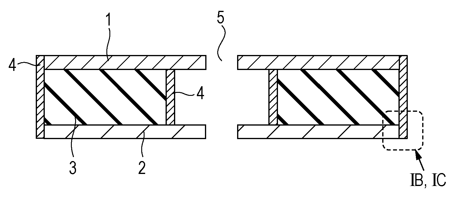
[0024]FIG. 1A is a cross-sectional view showing the configuration of a charged-particle beam lens of a first embodiment; FIG. 1B is an enlarged view of an area IB enclosed by the dotted line in FIG. 1A; and FIG. 1C is an enlarged view of an area IC in the case where the embodiments may not be applied. A plate-like anode 1 and cathode 2 may have sufficient electrical conductivity and may be made of metal or a semiconductor, whose volume resistivity is preferably 1×10³ [Ω·cm] or less. A plate-like insulator 3 is formed of glass or ceramic. At least the anode 1 is disposed on one of the surfaces of the insulator 3, and at least the cathode 2 is disposed on the opposite surface.

[0025]A high-resistance film 4 has a resistant value larger than the resistant values of the anode 1 and the cathode 2 and is formed of metal oxide, semiconductor oxide, metal nitride, or semiconductor nitride. The high-resistance film 4 has a resistant value that allows the potential difference between the catho...

second embodiment

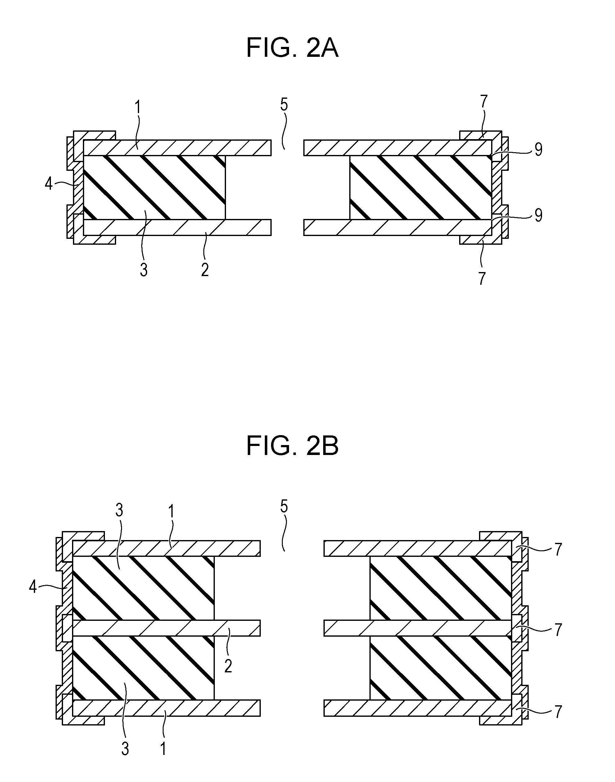
[0032]Next, a second embodiment will be described using FIGS. 2A and 2B. FIG. 2A is a cross-sectional view showing the configuration of a charged-particle beam lens of the second embodiment. In the second embodiment, electroconductive films 7 are formed on the anode 1 and the cathode 2 of the first embodiment. Although the electroconductive films 7 are disposed at least between the anode 1 and the high-resistance film 4 and between the cathode 2 and the high-resistance film 4, the electroconductive films 7 may be configured to cover the anode 1 and the cathode 2.

[0033]The electroconductive films 7 are formed of metal or a semiconductor, whose volume resistivity is 1×10³ [Ω·cm] or less. The high-resistance films 4 contain the same kind of element as that of the electroconductive film 7 but differs in resistant value from the electroconductive film 7, and the volume resistivity of the high-resistance film 4 is 1×10⁴ [Ω·cm] or more and 1×10¹⁴ [Ω·cm] or less, preferably, 1×10⁹ [Ω·cm] or...

third embodiment

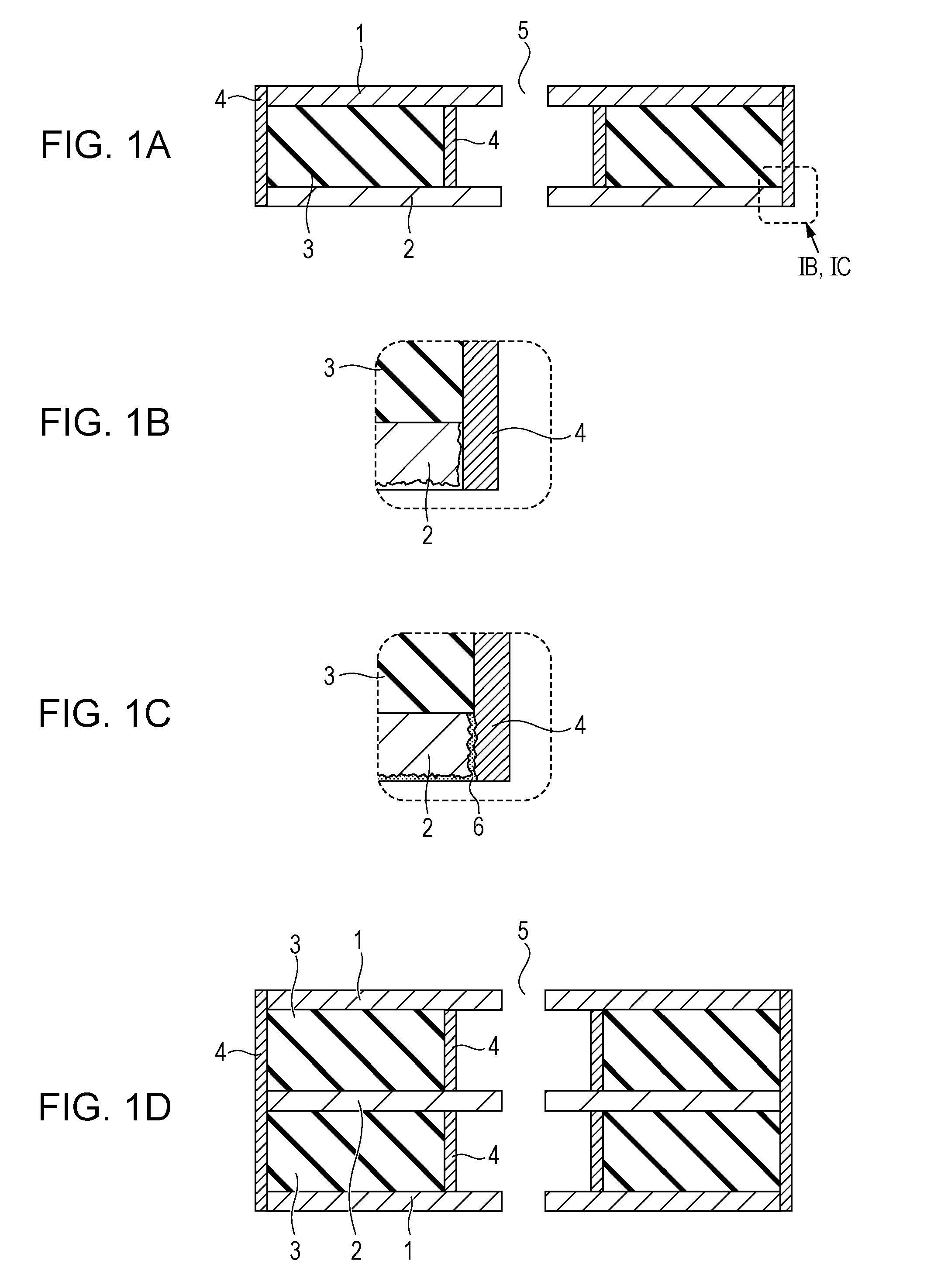
[0036]Next, a third embodiment will be described using FIGS. 3A to 3D. FIG. 3A is a cross-sectional view showing the configuration of a charged-particle beam lens of the third embodiment. FIG. 3B is an enlarge view of an area IIIB enclosed by the dotted line in FIG. 3A (the high-resistance film 4 is not shown). In this embodiment, an outer peripheral side a of the anode 1 is disposed inside an outer peripheral side c of the cathode 2 and an outermost side b of the insulator 3 (at the through-hole 5 side).

[0037]The electrostatic charged-particle beam lens has a configuration in which electrodes are layered, with an insulator therebetween, in which the boundary between a vacuum region, the insulator, and the electrodes is the triple junction 9. When an electric field is applied between the electrodes, creeping discharge tends to occur on the surface of the insulator due to electron emission from the cathode-side triple junction 9 due to an electric field concentration effect, a second...


PUM


Abstract

A charged-particle beam lens includes a plate-like anode, a plate-like cathode, and an insulator disposed between the anode and the cathode. The insulator, the anode, and the cathode have a passage portion through which a charged beam is passed. A high-resistance film is formed on an inner side of the insulator, the inner side forming the passage portion, or an outermost side of insulator, and the anode and the cathode are electrically connected together via the high-resistance film. The anode and the high-resistance film, and the cathode and the high-resistance film each contain the same metal or semiconductor element and have different resistant values. This suppresses electric field concentration due to an increase in resistance and poor connection at the interface between the anode and the cathode and the high-resistance film or at the interface between the electroconductive film and the high-resistance film, thus suppressing generation of discharge.

Description

BACKGROUND OF THE INVENTION[0001]1. Field of the Invention[0002]One disclosed aspect of the embodiments relates to the technical field of a charged particle beam optical system for use in an apparatus using a charged particle beam, and in particular, to a charged-particle beam lens for use in an exposure apparatus.[0003]2. Description of the Related Art[0004]Electron-beam exposure apparatuses use an electro-optical device for controlling the optical characteristics of an electron beam. There are two types of electron lens, that is, an electromagnetic type and an electrostatic type. The electrostatic type is suitable for size reduction because there is no need to provide a coil core, as compared with the electromagnetic type.[0005]On the other hand, a multibeam system in which a pattern is drawn with a plurality of electron beams without using a mask is one known electron-beam exposure technique. Since the number of beams in the multibeam system corresponds to the number of arrays of...

Claims


Application Information

Patent Timeline
Patent Type & Authority Patents(United States)
IPC IPC(8): H01J37/10H01J43/20H01J49/42
CPCH01J37/10H01J2237/038H01J3/18H01J37/12H01J2237/31774
Inventor SHIOZAWA, TAKASHI
Owner CANON KK
Why Eureka
Try Eureka