Semiconductor structure and method of forming the same

A semiconductor and conductive material layer technology, which is applied in semiconductor devices, semiconductor/solid-state device manufacturing, and semiconductor/solid-state device components, etc., can solve the problems of complex preparation steps, restrict development, and limit the flexibility of electronic equipment, and achieve small size, Easy-to-control, simple-structured effects

Inactive Publication Date: 2018-09-04
SHANGHAI INTEGRATED CIRCUIT RES & DEV CENT
View PDF4 Cites 0 Cited by
  • Summary
  • Abstract
  • Description
  • Claims
  • Application Information

AI Technical Summary

Problems solved by technology

[0002] In recent years, flexible, bendable and lightweight electronic devices and devices have received widespread attention. However, most of the devices used in these flexible electronic devices are traditional bulk hard devices, and the preparation steps are complicated. Limits the flexibility of electronic devices, thereby limiting their development in wearable electronics and related fields

Method used


Image

  • Semiconductor structure and method of forming the same
  • Semiconductor structure and method of forming the same
  • Semiconductor structure and method of forming the same

Examples


Embodiment Construction

[0041] The specific implementation manner of the present invention will be described in more detail below with reference to schematic diagrams. Advantages and features of the present invention will be apparent from the following description and claims. It should be noted that all the drawings are in a very simplified form and use imprecise scales, and are only used to facilitate and clearly assist the purpose of illustrating the embodiments of the present invention.

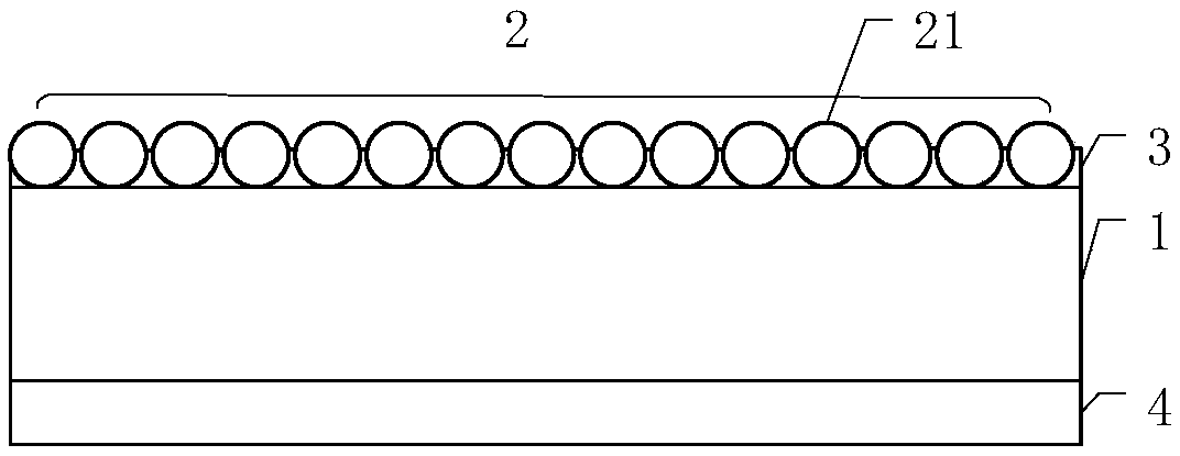
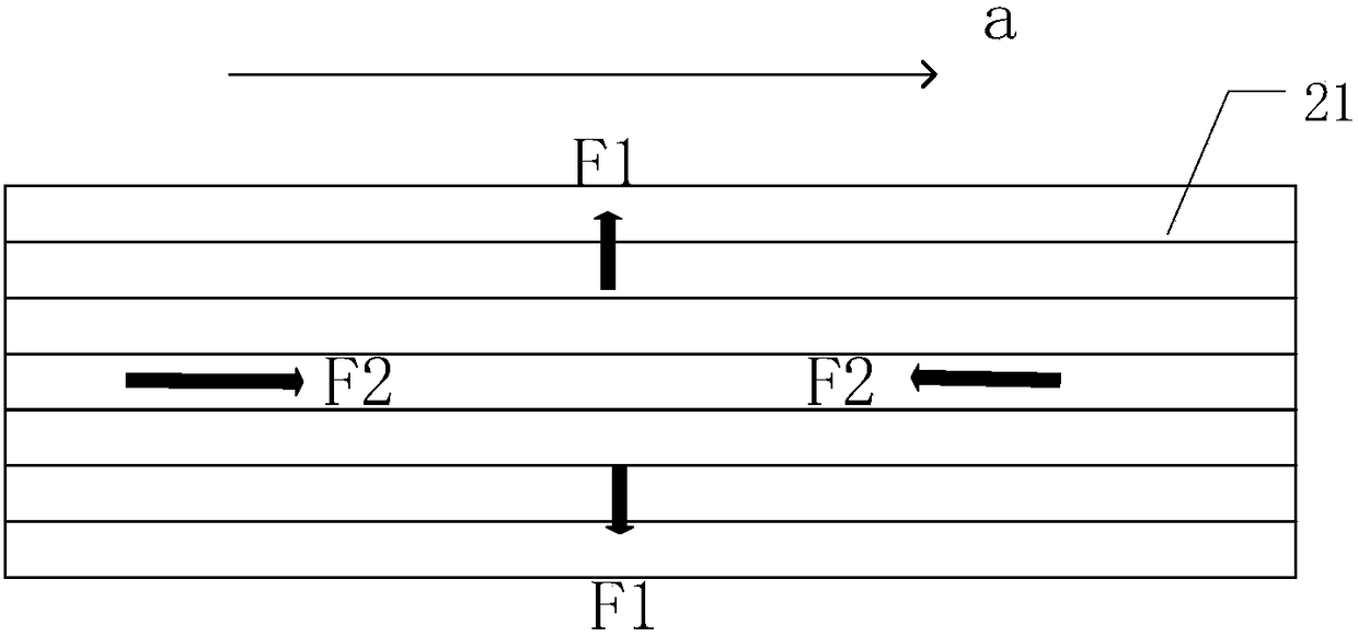
[0042] see figure 1 , which is a schematic diagram of the semiconductor structure provided in this embodiment, such as figure 1 As shown, the semiconductor structure includes a flexible substrate 1; an ester material layer 3, the ester material layer 3 is arranged on the flexible substrate 1, and the thermal expansion coefficient of the ester material layer 3 is greater than that of the flexible substrate The coefficient of thermal expansion of 1; the aligned carbon nanotube film 2, the aligned carbon nanotube ...


PUM

PropertyMeasurementUnit
thicknessaaaaaaaaaa

Abstract

The invention provides a semiconductor structure and a method of forming the same. When the semiconductor structure is heated or exposed to light, bending of a flexible substrate is promoted by an ester material layer and carbon nano tubes because the thermal expansion coefficient of the ester material layer is larger than that of the flexible substrate. Furthermore, the gaps between the flexiblesubstrate and the carbon nano tubes and gaps between the carbon nano tubes are filled with the ester material layer, so that the spaces between the carbon nano tubes are increased by the ester material layer. The carbon nano tubes can constrain the expansion of the ester material layer, so that the semiconductor structure is bent; and when not being heated or exposed to light, the semiconductor structure becomes flat again. The semiconductor structure having advantages of small size, simple structure, and great convenience in controlling can be applied to various devices like a switch or a sensor.

Description

technical field [0001] The invention relates to the field of semiconductor manufacturing, in particular to a semiconductor structure and a forming method thereof. Background technique [0002] In recent years, flexible, bendable and lightweight electronic devices and devices have received widespread attention. However, most of the devices used in these flexible electronic devices are traditional bulk hard devices, and the preparation steps are complicated. The flexibility of electronic devices is limited, thereby limiting its development in wearable electronics and related fields. Therefore, the prior art still needs to be improved and developed. Contents of the invention [0003] The object of the present invention is to provide a semiconductor structure and a forming method thereof, so as to improve the performance of existing flexible electronic devices. [0004] In order to achieve the above object, the present invention provides a semiconductor structure, which comp...

Claims


Application Information

Patent Timeline
Patent Type & Authority Applications(China)
IPC IPC(8): H01L23/14B81B7/00B81C1/00H01L21/50
CPCB81B7/00B81C1/00349H01L21/50H01L23/14
Inventor 武青青胡少坚朱建军
Owner SHANGHAI INTEGRATED CIRCUIT RES & DEV CENT
Why Eureka
Try Eureka