Embedded touch control panel and manufacturing method thereof

A technology of touch panel and manufacturing method, applied in the directions of optics, instruments, electrical components, etc., can solve the problems of large step difference between the edge of the first conductive layer COM and the flat layer JAS, broken wires, broken wires of bridge wires, etc., to achieve easy solution The effect of disconnection

Inactive Publication Date: 2018-09-04
NANJING CEC PANDA FPD TECH CO LTD
View PDF5 Cites 1 Cited by
  • Summary
  • Abstract
  • Description
  • Claims
  • Application Information

AI Technical Summary

Problems solved by technology

[0004] In the implementation of the existing In-cell touch panel solution, when the first conductive layer COM (ITO material) is etched, due to the difference in properties between its material ITO and the flat layer JAS, the ITO is etched to form an inverted taper, such as figure 2 As shown, it is easy to cause the bridge line formed by the second conductive layer PIX to be disconnected when the edge of the first conductive layer COM is covered; in addition, when the second insulating layer PAS2 is etched, the etching of the first conductive layer COM and the flat layer JAS The etch selection is relatively low, resulting in a large step difference between the edge of the first conductive layer COM and the flat layer JAS, which is likely to cause the bridge line formed by the second conductive layer PIX to break at this position, such as image 3 shown

Method used


Image

  • Embedded touch control panel and manufacturing method thereof
  • Embedded touch control panel and manufacturing method thereof
  • Embedded touch control panel and manufacturing method thereof

Examples


Embodiment 1

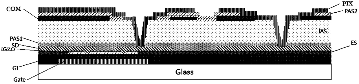
[0040] Figure 4-Figure 11 It is a schematic diagram of all steps of a manufacturing method of an in-cell touch panel of the present invention, as shown in the figure, the manufacturing method includes the following:

[0041] Step 1, forming a first metal layer on a substrate (Glass), the first metal layer is etched to form a scan line (not shown) and a gate (Gate), and the gate (Gate) is connected to the scan line, such as Figure 4 shown.

[0042] Step 2, firstly form a gate insulating layer GI covering the first metal layer, and then form a semiconductor layer (IGZO) on the gate insulating layer GI and set it opposite to the gate (Gate), such as Figure 5 shown.

[0043] Specifically, such as Image 6 As shown, wherein step 2 further includes the steps of: forming an etch barrier layer (ES) above the semiconductor layer (IGZO), and forming a first contact hole and a second contact hole on the etch barrier layer (ES); The first contact hole and the second contact hole ar...


PUM


Abstract

The invention discloses an embedded touch control panel and a manufacturing method thereof. The method comprises the steps that a first metal layer, a semiconductor layer, a second metal layer, a first insulating layer, a flat layer, a first conductive layer, a second insulating layer and a second conductive layer are formed successively; the apertures of first and second holes in the second insulating layer are lower than the aperture of a common electrode hole in the first conductive layer, the second insulating layer covers the first conductive layer completely, a third hole is formed in the second insulating hole, and the first conductive layer is electrically connected with the second conductive layer via the third hole. Thus, the problem that the second conductive layer PIX tends tobreakage is solved effectively.

Description

technical field [0001] The invention relates to the field of liquid crystal display, in particular to an embedded touch panel and a manufacturing method thereof. Background technique [0002] With the development of mobile terminals, the use of touch panels has become more and more extensive, and In-Cell touch is currently the most cutting-edge touch technology. In-cell touch is mainly divided into two categories: mutual capacitance and self-capacity, but almost all solutions need to add a touch layer, which needs to be added on the basis of the original design. Process debugging is required. [0003] figure 1 It is a cross-sectional view of an existing In-cell touch panel, including: a gate Gate, a gate insulating layer GI covering the gate Gate, a semiconductor layer IGZO located on the gate insulating layer GI, and a semiconductor layer located on the semiconductor layer IGZO. The etch stop layer ES, the source and drain SD and the touch signal line on the etch stop la...

Claims


Application Information

Patent Timeline
Patent Type & Authority Applications(China)
IPC IPC(8): H01L27/12G02F1/1333
CPCG02F1/13338H01L27/1214H01L27/1259
Inventor 胡威威高威易志根李彦柏舒强
Owner NANJING CEC PANDA FPD TECH CO LTD
Why Eureka
Try Eureka