
A driving timing control method of frame transfer type area array ccd

A technology of driving timing and control method, applied in the parts of color TV, parts of TV system, TV, etc., can solve the problems of small adjustable range of exposure time, insufficient charge transfer, poor signal integrity, etc. Imaging cycle, optimize imaging performance, improve the effect of frame rate

Inactive Publication Date: 2020-11-06
NAT SPACE SCI CENT CAS
View PDF5 Cites 0 Cited by
  • Summary
  • Abstract
  • Description
  • Claims
  • Application Information

AI Technical Summary

Problems solved by technology

Although imaging is possible, there are the following problems: due to insufficient charge transfer in the imaging area, there are residual charges in the imaging area after the image transfer of the previous frame, and there is no charge clearing operation in the basic driving sequence, and these residual charges will affect the next frame as noise Imaging, reducing the signal-to-noise ratio; the timing of charge dumping dumps residual charges by adding a transfer and readout between two effective imaging cycles, but the imaging cycle is long and the frame rate is slow; the adjustable range of exposure time is small , requires an external mechanical shutter; only the charge in the effective photosensitive area is transferred, and the signal integrity is poor

Method used


Image

  • A driving timing control method of frame transfer type area array ccd
  • A driving timing control method of frame transfer type area array ccd
  • A driving timing control method of frame transfer type area array ccd

Examples


Embodiment Construction

[0020] The present invention will be described in detail below in conjunction with the accompanying drawings and specific embodiments, but it is not intended to limit the present invention.

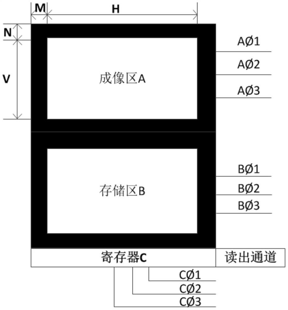
[0021] The device structure of the instrument "frame transfer type area array CCD" applicable to the present invention is as attached figure 1 As shown, according to different functions, it is divided into: imaging area A, which accepts incident light exposure and generates photogenerated charges. The effective photosensitive area is the middle white area, which contains a total of H*V photosensitive pixels. Each M column is symmetrical, and each N row is symmetrical up and down; the storage area B has the same structure as the imaging area A, except that it does not receive light and is only used to store the charge transferred from the imaging area A; register C includes H+2*M A register unit is used to store a row of charges transferred from the storage area B; the readout channel, the...


PUM


Abstract

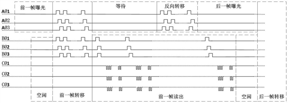
The invention discloses a frame transfer type area array CCD driving timing control method, the frame transfer type area array CCD includes: an imaging area A for exposing and generating charges; a storage area B for storing the data transferred from the imaging area A Charge; register C, used to register a row of charges transferred from storage area B; readout channel, read out the charges in register C one by one; areas A, B, and C each include three driving clock pins; the method Including: the controller is controlled to be normally low for exposure; the controller sends pulses of a specific order and number to and for frame transfer; the controller sends pulses of a specific order and number to and for frame readout, and then the controller is normally low , is normally high, enters the idle state before the next frame transfer, and at the same time the controller is first controlled to be normally low, enters the waiting state, and then sends a specific sequence and number of pulses to the reverse transfer to clear the residual charge and the light generated during the waiting period charge.

Description

technical field [0001] The invention relates to the technical field of photoelectric imaging, in particular to a method for controlling the drive sequence of a frame transfer type area array CCD. Background technique [0002] In the field of optoelectronic imaging, a Charge Coupled Device (CCD) is a commonly used imaging device, which converts incident light into a certain number of charges according to the semiconductor photoelectric effect, and then converts it into a measurable voltage or current through a processing circuit. Then inversely deduce the incident light intensity. According to the different pixel arrangement structure, CCD can be divided into two types: line array and area array, and area array CCD can be divided into full frame transfer type, frame transfer type and interline transfer type according to the different charge transfer methods. [0003] Frame transfer type area array CCD has become the first choice of CCD imaging device due to its large fill fa...

Claims


Application Information

Patent Timeline
Patent Type & Authority Patents(China)
IPC IPC(8): H04N5/372
CPCH04N25/713H04N25/71
Inventor 梁少林王咏梅贾楠石恩涛
Owner NAT SPACE SCI CENT CAS
Learn More