Method for manufacturing multi-layer thick-copper circuit board

A manufacturing method and circuit board technology, applied in multilayer circuit manufacturing, printed circuit manufacturing, printed circuit and other directions, can solve problems such as unfavorable reliability of thick copper circuit boards, hidden dangers of delaminated boards, and poor adhesion between substrates and prepregs, etc. problems, to improve the one-time yield and product reliability, solve the board surface depression, and improve the appearance quality of the effect

Inactive Publication Date: 2018-09-04
SHENZHEN KINWONG ELECTRONICS
View PDF8 Cites 7 Cited by
  • Summary
  • Abstract
  • Description
  • Claims
  • Application Information

AI Technical Summary

Problems solved by technology

[0004] The purpose of the present invention is to provide a method for making a multi-layer thick copper circuit board to solve the problem of the base material and prepreg at the bottom of the copper-free area of ​​the thick copper core board when the copper thickness of the thick copper core board is greater than or equal

Method used


Image

  • Method for manufacturing multi-layer thick-copper circuit board
  • Method for manufacturing multi-layer thick-copper circuit board
  • Method for manufacturing multi-layer thick-copper circuit board

Examples


Embodiment Construction

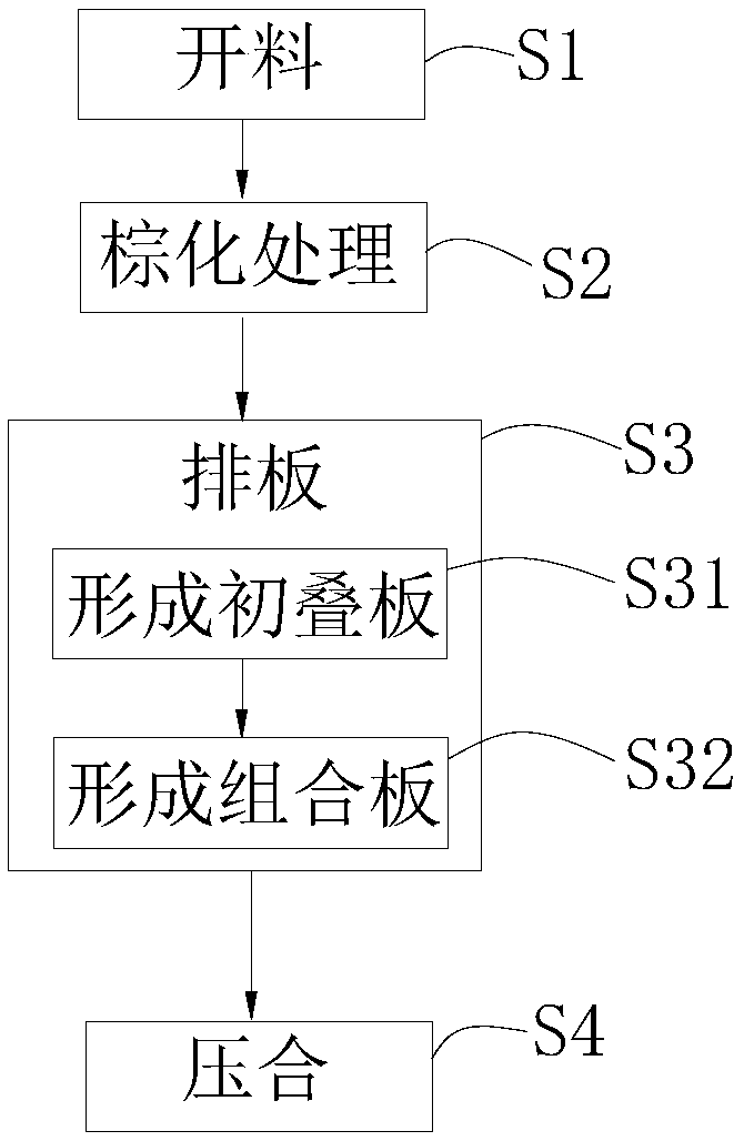
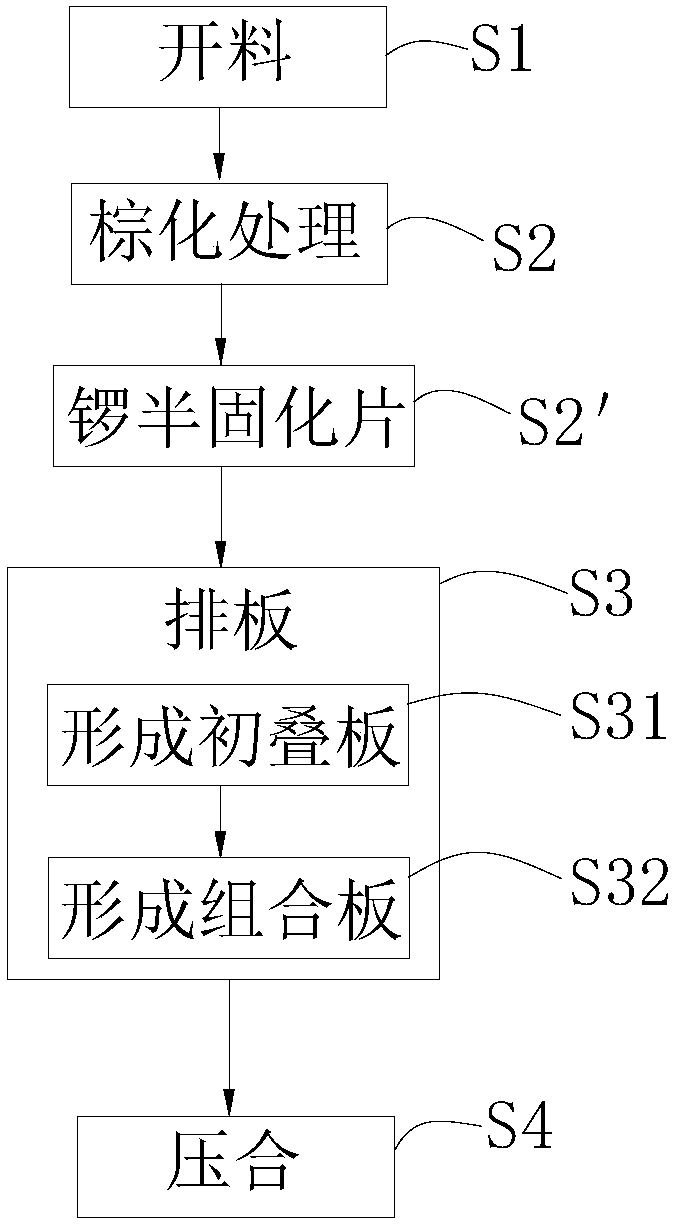
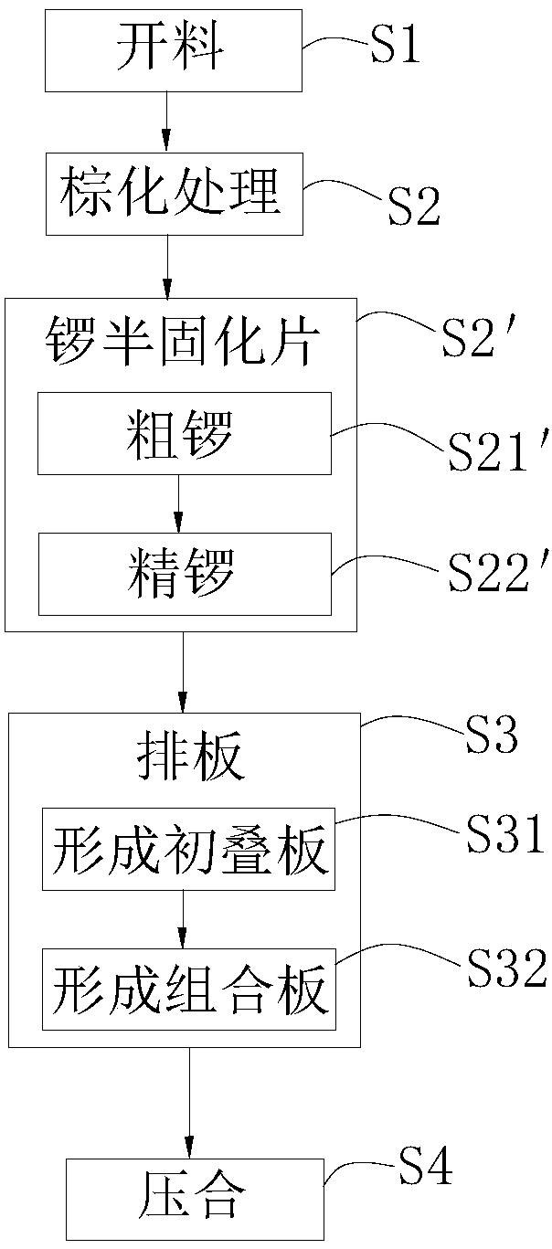
[0038] In order to make the object, technical solution and advantages of the present invention clearer, the present invention will be further described in detail below in conjunction with the accompanying drawings and embodiments. It should be understood that the specific embodiments described here are only used to explain the present invention, not to limit the present invention.

[0039] It should be noted that when an element is referred to as being “fixed” or “disposed on” another element, it may be directly on the other element or it may be indirectly fixed or disposed on the other element through a third component. When an element is referred to as being "connected to" another element, it can be directly connected to the other element or it can be indirectly connected to the other element through a third element.

[0040] It is to be understood that the terms "length", "width", "top", "bottom", "front", "rear", "left", "right", "vertical", "horizontal", "top" , "bottom"...


PUM

PropertyMeasurementUnit
Thicknessaaaaaaaaaa

Abstract

The invention relates to the technical field of multi-layer circuit board manufacturing, in particular to a method for manufacturing a multi-layer thick-copper circuit board. The method comprises steps of rough shape cutting, browning processing, board layout, and pressing. Organic glass cloth prepregs are combined with non-woven prepregs; and the two surfaces of all thick copper boards face the non-woven prepregs. During the pressing process, solidified liquid of the non-woven prepregs flow into copper-free regions of the corresponding thick copper core boards fully, so that the binding forces of the bases of the bottoms of the copper-free regions and the prepregs are strengthened; adhesive filling is carried out fully; hole occurrence is avoided; and potential safety hazards of layeringand board explosion due to heating are prevented effectively. The organic glass cloth prepregs serve as strength supports between the thick copper core plate and the outer copper foils and the adjacent thick copper core plate are combined, so that problems of board surface recession, wrinkling, and sliding and the like are solved; the laminated multi-layer copper board has the uniform thickness; the appearance quality of the laminated board is improved; and the good foundation is laid for follow-up film pasting, electroplating and SMT assembling.

Description

technical field [0001] The invention belongs to the technical field of multilayer circuit board manufacture, and more specifically relates to a method for manufacturing a multilayer thick copper circuit board. Background technique [0002] Multi-layer circuit board lamination refers to stacking prepreg (PP for short) between any adjacent two-layer circuit boards and combining them together under high temperature and high pressure. In order to meet the needs of power modules, automotive electronics, etc. to carry large current 1. The power supply is stable and needs better heat dissipation products. Therefore, thick copper circuit boards are favored. When thick copper circuit boards are thicker (≥4OZ), there are many difficulties in the lamination process. [0003] Pressing is to use high temperature and high pressure to heat and melt the prepreg, and make the melted liquid glue flow, and then transform into a solidified sheet, so as to bond one or more thick copper core boar...

Claims


Application Information

Patent Timeline
IPC IPC(8): H05K3/46
CPCH05K3/4611H05K2203/0228
Inventor 曾向伟张传超谢伦魁张霞盘燕明
Owner SHENZHEN KINWONG ELECTRONICS
Why Eureka
Try Eureka