Solid-state imaging device, method for manufacturing solid-state imaging device, and electronic apparatus
A solid-state imaging device and optoelectronic technology, which is applied to electric solid-state devices, radiation control devices, televisions, etc., can solve the problems of deterioration of conversion efficiency, increase of capacitance of charge-voltage conversion part, deterioration of noise characteristics, etc., and achieve the effect of high sensitivity
- Summary
- Abstract
- Description
- Claims
- Application Information
AI Technical Summary
Problems solved by technology
Method used
Image

Examples
no. 1 Embodiment approach
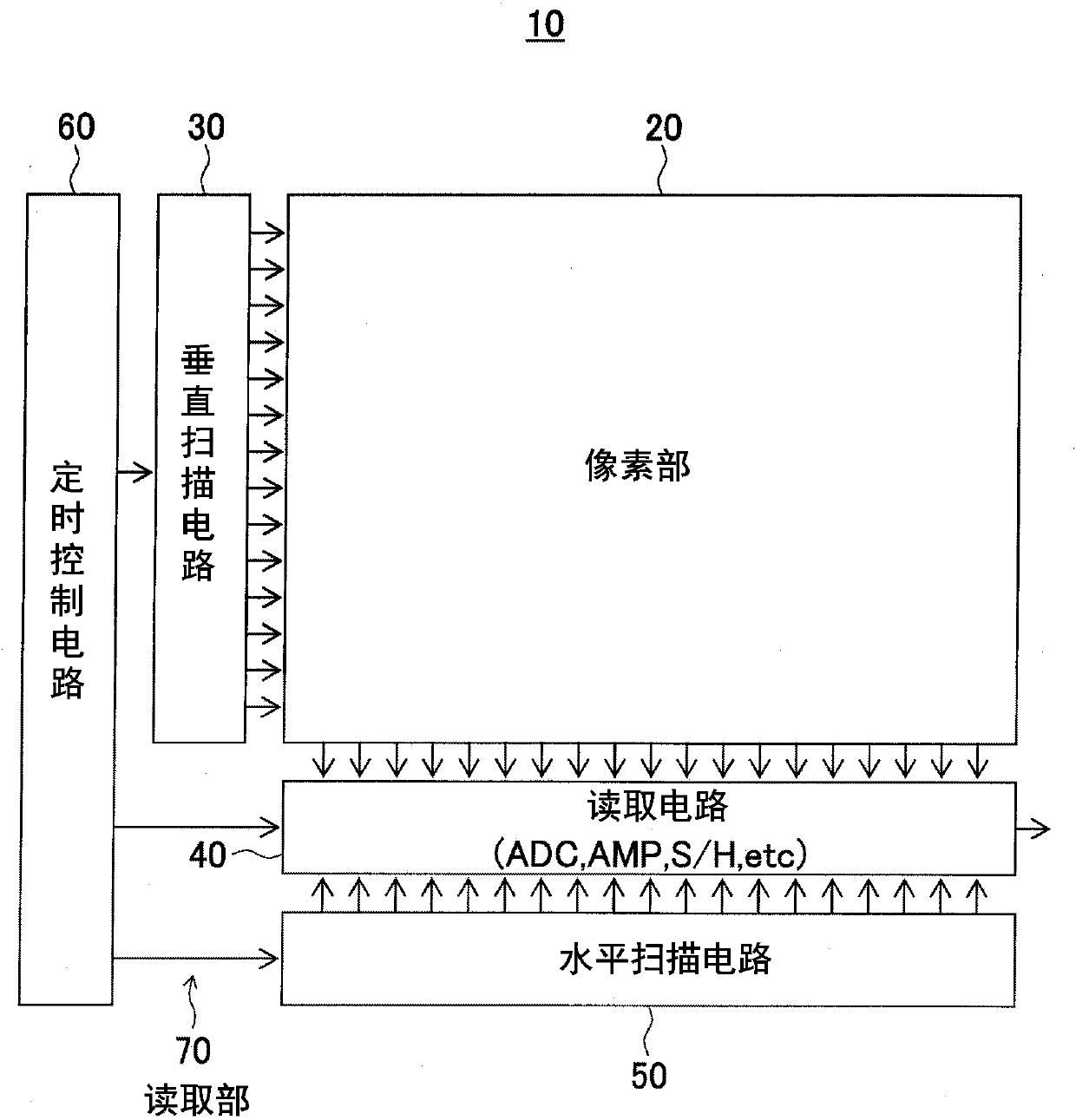
[0081] figure 1 It is a block diagram showing a configuration example of the solid-state imaging device according to the first embodiment of the present invention.
[0082] In this embodiment, the solid-state imaging device 10 is constituted by, for example, a CMOS image sensor.
[0083] Such as figure 1 As shown, the solid-state imaging device 10 has as main components: a pixel unit 20 as an imaging unit; a vertical scanning circuit (row scanning circuit) 30; a reading circuit (column reading circuit) 40; a horizontal scanning circuit (column scanning circuit) 40; circuit) 50; and a timing control circuit 60.
[0084] Among these components, for example, the vertical scanning circuit 30, the reading circuit 40, the horizontal scanning circuit 50, and the timing control circuit 60 constitute a pixel signal reading unit 70.
[0085] In the first embodiment, as will be described in detail later, the solid-state imaging device 10 has pixels (or pixel portions 20) arranged in a...
no. 2 Embodiment approach
[0299] Figure 19 It is a schematic cross-sectional view showing a configuration example of main parts of the embedded photodiode (PPD) according to the second embodiment of the present invention, except for the charge transfer gate portion.
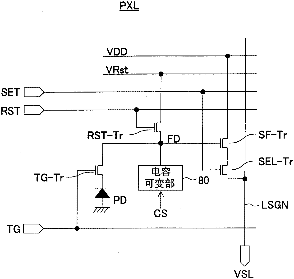
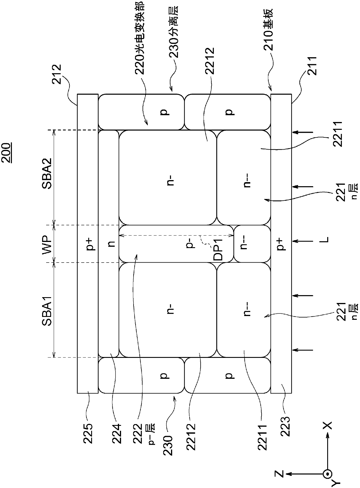
[0300] The embedded photodiode (PPD) 200A of the second embodiment and the embedded photodiode (PPD) 200 of the first embodiment ( image 3 ) are as follows.
[0301] In the photoelectric conversion portion 220 of the embedded photodiode (PPD) 200 of the first embodiment, the p-layer of the second conductivity type (in image 3 In the example of the p-layer) 222 has a given width WP in the direction X perpendicular to the normal line of the substrate 210, and has a width from the n layer (first conductivity type semiconductor layer) 221 in the normal direction Z of the substrate The depth DP1 from the surface on the second substrate surface 212 side does not reach the surface on the first substrate surface 211 side.
[0302] On the ot...
no. 3 Embodiment approach
[0307] Figure 20 It is a schematic cross-sectional view showing a configuration example of main parts of the embedded photodiode (PPD) according to the third embodiment of the present invention, except for the charge transfer gate portion.
[0308] The embedded photodiode (PPD) 200B of the third embodiment and the embedded photodiode (PPD) 200 of the first embodiment ( image 3 ) are as follows.
[0309] In the photoelectric conversion portion 220 of the embedded photodiode (PPD) 200 of the first embodiment, the p-layer of the second conductivity type (in image 3 In the example of the p-layer) 222 has a given width WP in the direction X perpendicular to the normal line of the substrate 210, and has a width from the n layer (first conductivity type semiconductor layer) 221 in the normal direction Z of the substrate The depth DP1 from the surface on the second substrate surface 212 side does not reach the surface on the first substrate surface 211 side.
[0310] On the othe...
PUM
 Abstract
Description
Claims
Application Information
 - R&D
- Intellectual Property
- Life Sciences
- Materials
- Tech Scout
- Unparalleled Data Quality
- Higher Quality Content
- 60% Fewer Hallucinations
Browse by: Latest US Patents, China's latest patents, Technical Efficacy Thesaurus, Application Domain, Technology Topic, Popular Technical Reports.
© 2025 PatSnap. All rights reserved.Legal|Privacy policy|Modern Slavery Act Transparency Statement|Sitemap|About US| Contact US: help@patsnap.com