
PCB fixing and redundancy connection structure of integration circuit chip capable of repeat plugging

An integrated circuit and redundant connection technology, which is applied in the field of PCB fixing and redundant connection structures, can solve the problems of weak anti-vibration ability, singleness, and difficulty in ensuring reliable contact between integrated circuit pins and tube sockets, so as to reduce bending stress , The effect of improving the overall fatigue life

Active Publication Date: 2018-09-07
CHINA NORTH ENGINE INST TIANJIN
View PDF6 Cites 0 Cited by
  • Summary
  • Abstract
  • Description
  • Claims
  • Application Information

AI Technical Summary

Problems solved by technology

[0003] The integrated circuits installed on the PCB of electronic control products are roughly divided into two types, one can be directly soldered to the PCB, and its anti-vibration ability is strong; the other is due to the confidentiality of intellectual property rights, and cannot be directly soldered to the PCB. The program chip needs to be connected by a re-pluggable tube socket, which has weak anti-vibration ability
[0004] The traditional method of PCB fixing of re-pluggable integrated circuit chips adopts a single integrated circuit socket connection method. This connection method only relies on the locking pressure of the socket's own locking device to ensure contact reliability, but due to Without welding, it is difficult to ensure reliable contact between the IC pins and the socket

Method used


Image

  • PCB fixing and redundancy connection structure of integration circuit chip capable of repeat plugging
  • PCB fixing and redundancy connection structure of integration circuit chip capable of repeat plugging
  • PCB fixing and redundancy connection structure of integration circuit chip capable of repeat plugging

Examples


Embodiment Construction

[0023] It should be noted that, in the case of no conflict, the embodiments of the present invention and the features in the embodiments can be combined with each other.

[0024] The present invention will be described in detail below with reference to the accompanying drawings and examples.

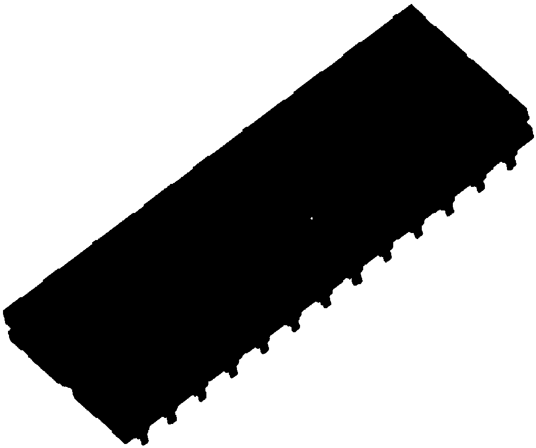
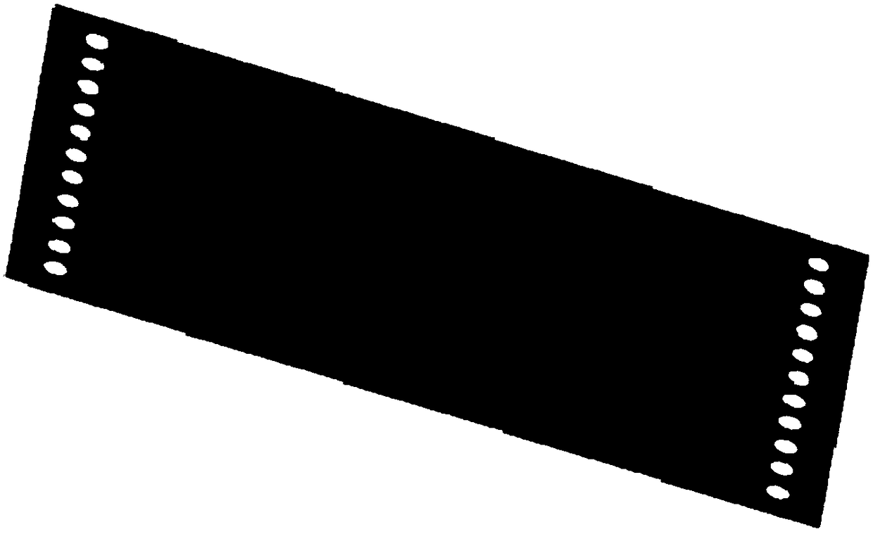
[0025] A PCB fixation and redundant connection structure for re-pluggable integrated circuit chips, such as Figures 1 to 6 As shown, it includes an integrated circuit socket 1 with a locking function, two flexible circuit boards 3 , two 90-degree single-row elbow pins 4 , and two 90-degree single-row elbow socket females 5 .

[0026] The integrated circuit socket 1 is welded on the PCB for fixing the integrated circuit 2; both ends of the integrated circuit socket 1 are respectively connected to a flexible circuit board 3, and the other end of the flexible circuit board 3 is connected to a 90-degree single The elbow end of the row of elbow pins 4, the other end of the 90-degree single-...


PUM


Abstract

The present invention provides a PCB fixing and redundancy connection structure of an integration circuit chip capable of repeat plugging. The structure comprises an integration circuit tube socket with a latching function, two flexible circuit boards, two 90-degree single-row bending head plugging buses and two 90-degree single-row bending head insertion pins. The integration circuit tube socketis welded on the PCB and is configured to fix the integration circuit; the two ends of the integration circuit tube socket are respectively connected with the two flexible circuit boards, the other ends of the flexible circuit boards are connected with the heading end ends of the two 90-degree single-row bending head insertion pins, the other ends of the two 90-degree single-row bending head insertion pins are plugged with the 90-degree single-row bending head plugging buses, and the 90-degree single-row bending head plugging buses are welded on the PCB. The PCB fixing and redundancy connection structure is reasonable in layout and design, employs the dual-directional redundancy connection technology to eliminate bad contact of pin signals of the integration circuit caused by vibration oftransverse and vertical directions, and employs the redundancy connection technology of signal transmission to ensure the reliable connection of the pins of the integration circuit and the PCB.

Description

technical field [0001] The invention belongs to the technical field of electronic control of military armored vehicles, and in particular relates to a PCB fixing and redundant connection structure for re-pluggable integrated circuit chips. Background technique [0002] All-weather and all-region are the basic requirements for the environmental adaptability of military armored vehicles. All electronic control products equipped on military armored vehicles are always faced with possible shock and vibration due to the road environment. Strong shocks and vibrations often lead to poor contact between some non-welded integrated circuit chips and the motherboard PCB signal, resulting in the failure of the control function of electronic control products. It is particularly important to carry out anti-vibration design on key chips of electronic control products. [0003] The integrated circuits installed on the PCB of electronic control products are roughly divided into two types, o...

Claims


Application Information

Patent Timeline
Patent Type & Authority Applications(China)
IPC IPC(8): H05K1/02H05K1/14H05K1/18H01R12/71H01R12/79H01R13/02H01R33/74
CPCH01R12/716H01R12/79H01R13/02H01R33/74H05K1/0271H05K1/147H05K1/18H05K2201/10189
Inventor 杨俊恩闫云艳范燕朝董新宇李向荣智海峰张春胡勇和龙李菲菲张永青
Owner CHINA NORTH ENGINE INST TIANJIN
Learn More