A Method for Measuring Magnetization Dynamics at the Nanoscale

A nanoscale and measurement method technology, applied in the direction of magnetization measurement, magnetic performance measurement, etc., can solve the problems that the dynamic characteristics of nanoscale magnetization cannot be obtained, the imaging effect is easily limited by optical components, and the dynamic information of magnetization cannot be obtained, etc., to achieve The effect of fast test speed, long service life and simple device

Active Publication Date: 2020-08-28
嘉兴诺恩医疗科技有限公司
View PDF5 Cites 0 Cited by
  • Summary
  • Abstract
  • Description
  • Claims
  • Application Information

AI Technical Summary

Problems solved by technology

The magneto-optical Kerr effect measurement device mainly detects the magnetization observation of the sample surface by detecting the change of the polarization state of a beam of linearly polarized light after it is reflected on the surface of the material. Therefore, the imaging effect is easily limited by the optical elements. Technical defect 1: The spatial resolution of the traditional focusing Kerr microscope using microscope objective lens is determined by the optical diffraction limit, so it is impossible to obtain the dynamic characteristics of magnetization at the nanometer scale; the existing technical defect 2: it is impossible to obtain higher frequency magnetization in the sample. Magnetization dynamic information, the measurement method of the nanoscale magnetization dynamics can solve the problem

Method used


Image

  • A Method for Measuring Magnetization Dynamics at the Nanoscale
  • A Method for Measuring Magnetization Dynamics at the Nanoscale

Examples


Embodiment Construction

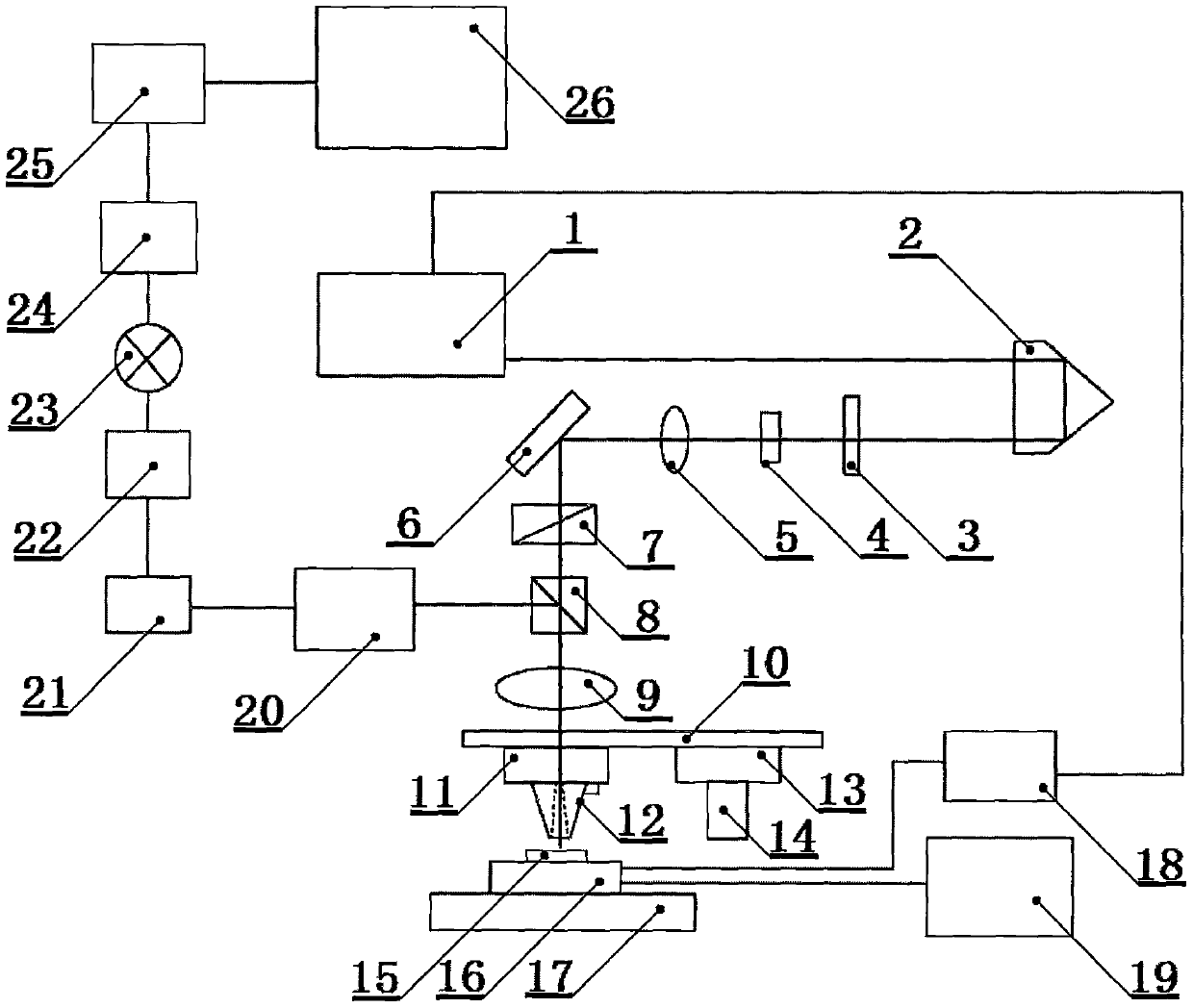
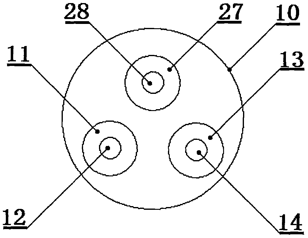
[0027] Such as figure 1 It is a schematic diagram of the present invention, the pulsed laser 1, signal generator 18, waveguide 16, and oscilloscope 19 are cable-connected in turn, and the optical bridge detector 20, bias tee 21, amplifier I22, mixer 23, amplifier II24, The analog-to-digital converter 25 and the computer 26 are cable-connected in turn, and the laser beam emitted by the pulsed laser 1 passes through the delayer 2, 1 / 4 wave plate 3, concave lens 4, convex lens 15, plane mirror 6, polarizer 7, and beam splitter successively. Device 8, convex lens II9, lens stage 10, atomic force microscope I11, probe I12, thereby forming an incident optical path, the reflected light generated by the laser beam irradiating on the surface of sample 15 passes through probe I12, atomic force microscope I11, lens stage 10, Convex lens II9 and beam splitter 8 form a reflected optical path, the reflected light is deflected to the optical bridge detector 20 by the beam splitter 8, the pro...


PUM


Abstract

The invention relates to the field of material surface magnetic measurement, in particular to a measurement method of nano-scale magnetization dynamics. A measurement device comprises a pulse laser, adelayer, a quarter wave plate, a concave lens, a convex lens I, a plane mirror, a polarizer, a beam splitter, a convex lens II, a lens table, an atomic force microscope I, a probe I, a lens holder, an objective lens, a sample, a waveguide, a sample table, a signal generator, an oscilloscope, a detector, a bias tee, an amplifier I, a mixer, an amplifier II, an analog-to-digital converter, a computer, an atomic force microscope II, a probe II and a phase-sensitive detector. A single nanostructure can be measured, measurement of magnetization dynamics on the sample surface can reach sub-micron spatial resolution, two different atomic force microscope tips are adopted for contact mode atomic force microscope scanning and near-field time-resolved magneto-optical Kerr effect experiment respectively, GHz-band magnetization dynamics on the sample surface are detected with a frequency domain method, and higher sensitivity is realized.

Description

technical field [0001] The invention relates to the field of material surface magnetic measurement, in particular to a nanoscale magnetization dynamic measurement method capable of measuring the high-frequency dynamic magnetization of a single nanostructure on the material surface. Background technique [0002] The magneto-optical Kerr effect measurement device is an important means in the study of material surface magnetism. Its working principle is based on the magneto-optic Kerr effect caused by the interaction between light and magnetized media. Magnetic detection, and non-contact measurement can be realized, and it has important applications in the research of magnetic order, magnetic anisotropy, interlayer coupling and phase transition behavior of magnetic ultrathin films. The magneto-optical Kerr effect measurement device mainly detects the magnetization observation of the sample surface by detecting the change of the polarization state of a beam of linearly polarized...

Claims


Application Information

Patent Timeline
Patent Type & Authority Patents(China)
IPC IPC(8): G01R33/12
CPCG01R33/1215
Inventor 张向平方晓华范晓雯
Owner 嘉兴诺恩医疗科技有限公司
Why Eureka
Try Eureka